Semiconductor memory device
- Summary
- Abstract
- Description
- Claims
- Application Information
AI Technical Summary
Benefits of technology
Problems solved by technology
Method used
Image

Examples
embodiment 1
[0101](Embodiment 1)
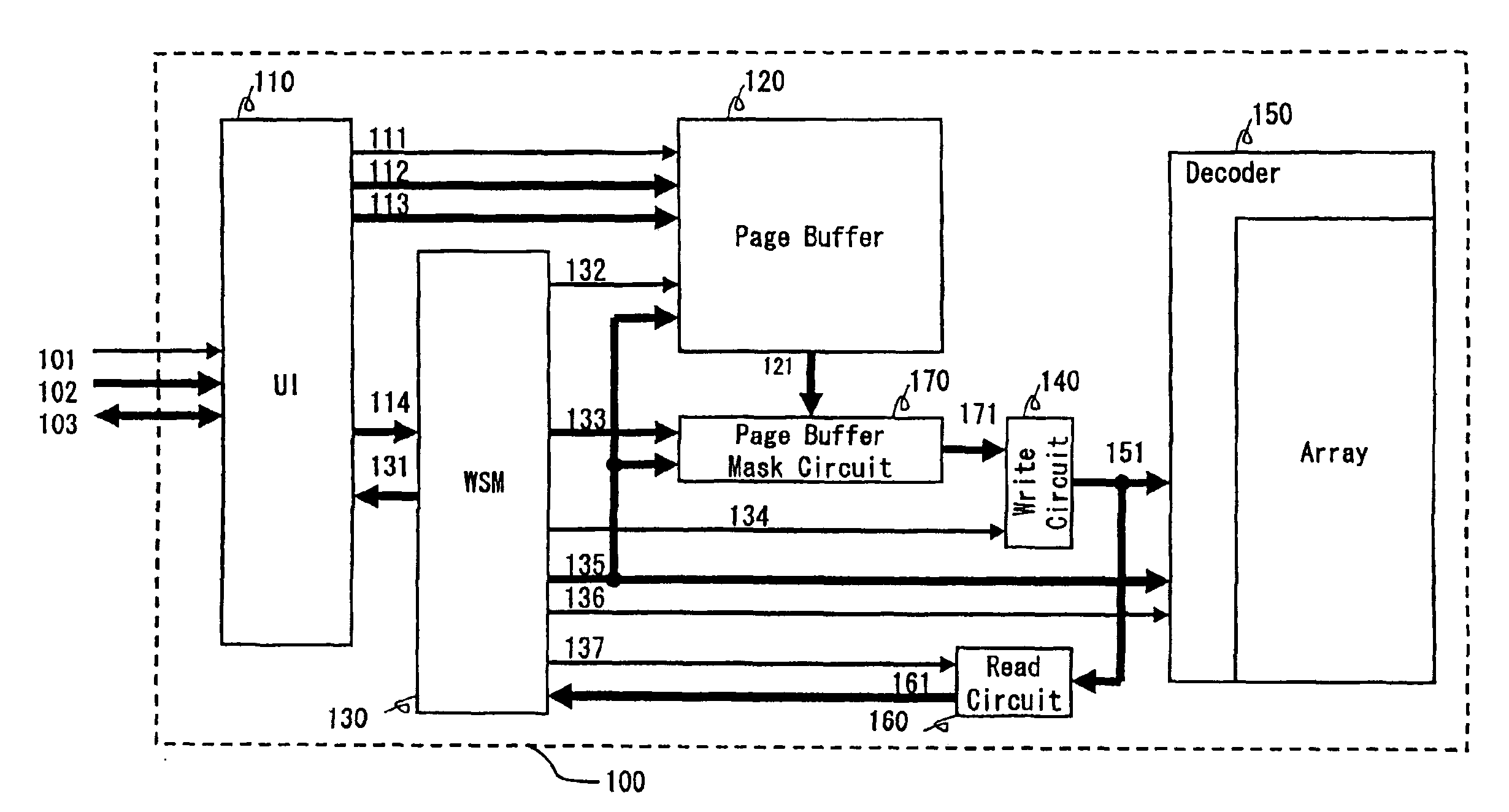
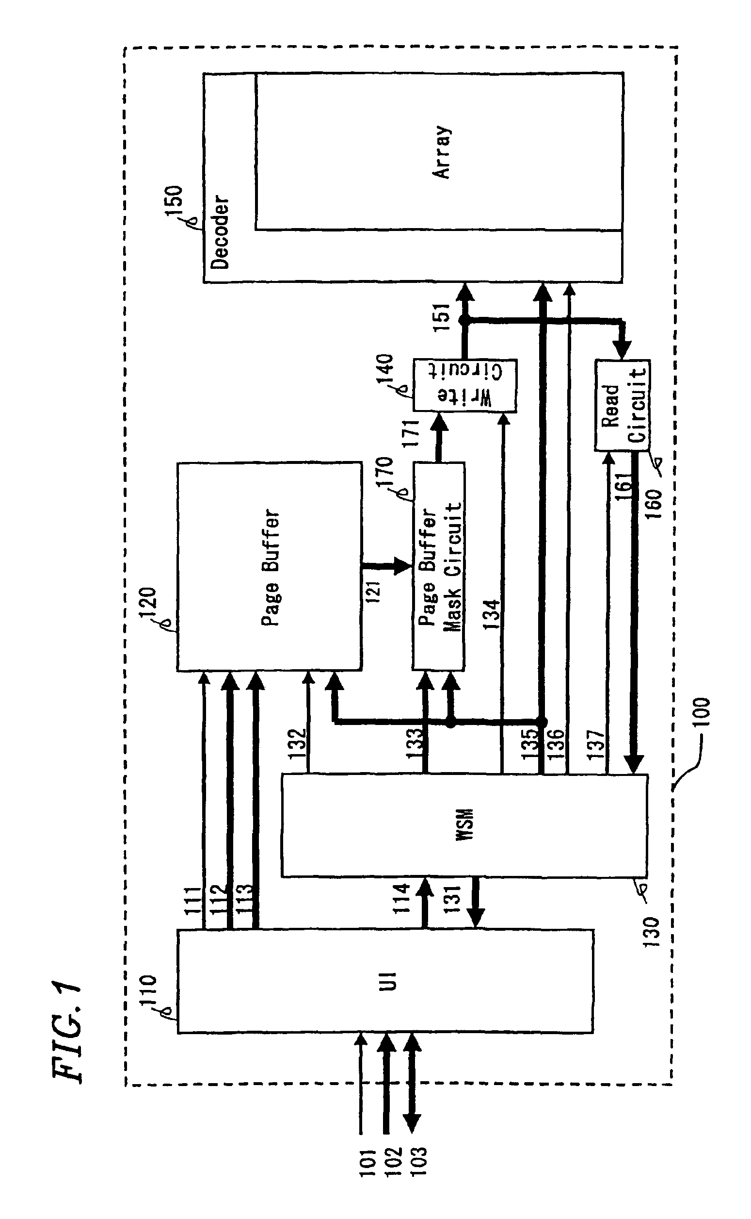
[0102]FIG. 1 is a block diagram showing a semiconductor memory device according to Embodiment 1 of the present invention. The semiconductor memory device of FIG. 1 is a flash memory 100 comprising a page buffer circuit 120. FIG. 1 shows portions of the flash memory 100 which are involved in write operations.
[0103]The flash memory 100 comprises a UI circuit 110, a page buffer circuit 120, a WSM circuit 130, a write control circuit 140, a memory array 150, a read circuit 160, and a page buffer mask circuit 170.
[0104]This flash memory 100 receives and outputs external control signals, address signals, and data signals from and to the outside via a control bus 101, an address bus 102 and a data bus 103, respectively.
[0105]In the flash memory 100, a write operation using the page buffer circuit 120 is performed in the following manner.
[0106]When a control signal indicating a write operation, an address signal indicating a write address, and a data signal indicating da...
embodiment 2
[0240](Embodiment 2)
[0241]FIG. 6 is a block diagram showing a semiconductor memory device according to Embodiment 2 of the present invention. FIG. 6 shows a flash memory 200 having a page buffer circuit as a semiconductor memory device. Portions of the flash memory 200, which are involved in writing, are shown in FIG. 6. Note like numerals indicate like parts in FIGS. 1 and 6.
[0242]The flash memory 200 is a multi-value flash memory 200.
[0243]The flash memory 200 comprises a UI circuit 110, a page buffer circuit 120, a WSM circuit 130, a write control circuit 140, a memory array 250, a read circuit 160, a page buffer mask circuit 170, and a data logic circuit 280.
[0244]In the flash memory 200, a write operation is performed using the page buffer circuit 120 as follows. Note that the description of a portion of the write operation common to the flash memory 100 of Embodiment 1 is omitted.
[0245]As compared to two-value flash memories, the multi-value flash memory 200 requires strict co...
embodiment 3
[0269](Embodiment 3)
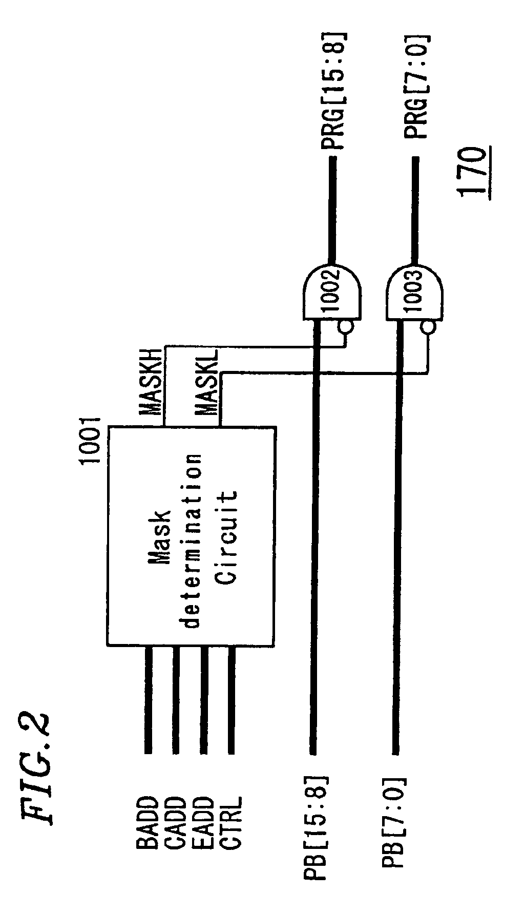
[0270]FIG. 8 is a circuit diagram showing an exemplary configuration of a page buffer mask circuit 270 in a flash memory according to Embodiment 3 of the present invention.
[0271]The page buffer mask circuit 270 comprises an address determination circuit 1001, AND circuits 1002 and 1003, and a deactivation circuit 4000 which deactivate a masking function.
[0272]Here, the address determination circuit 1001 is substantially the same as that which described in Embodiment 1 with reference to FIG. 2.
[0273]The deactivation circuit 4000 comprises AND circuits 4002 and 4003 and an inverter circuit 4004.
[0274]The page buffer mask circuit 270 can handle both the byte mode where data is processed on a byte-by-byte basis and the word mode where data is processed on a word-by-word basis, as in the page buffer mask circuit 170 described in Embodiment 1 with reference to FIG. 2. The mask determination circuit 1001 is used to control a masking function of masking the upper byte an...
PUM
 Abstract
Description
Claims
Application Information
 - R&D Engineer
- R&D Manager
- IP Professional
- Industry Leading Data Capabilities
- Powerful AI technology
- Patent DNA Extraction
Browse by: Latest US Patents, China's latest patents, Technical Efficacy Thesaurus, Application Domain, Technology Topic.
© 2024 PatSnap. All rights reserved.Legal|Privacy policy|Modern Slavery Act Transparency Statement|Sitemap