Image processor

a technology of image processing and processor, which is applied in the field of image processing, can solve the problems of power consumption as well as the chip size and the disadvantageous increase of manufacturing cost, and achieve the effect of reducing image processing time and cos

Active Publication Date: 2005-09-13
MEGACHIPS
View PDF6 Cites 25 Cited by
  • Summary
  • Abstract
  • Description
  • Claims
  • Application Information

AI Technical Summary

Benefits of technology

[0025]Accordingly, an object of the present invention is to provide an image processor capable of reducing an image processing time as w...

Problems solved by technology

However, the pixel size (pixel number) of the image pickup sensor 105 is not uniform.
When the capacity of the line memories is matched with a popular pixel size, therefore, the image processing in units of multiple pixels cannot be executed on an image sensor having a larger pixel size.
When the capacity of the line memories built into an image processing circuit integrated into a chip is increased, power consumption as well as the chip size and the manufacturing cost are disadvantageously increased.
Thus,...

Method used


Image

  • Image processor
  • Image processor
  • Image processor

Examples


embodiment 1

[0041]

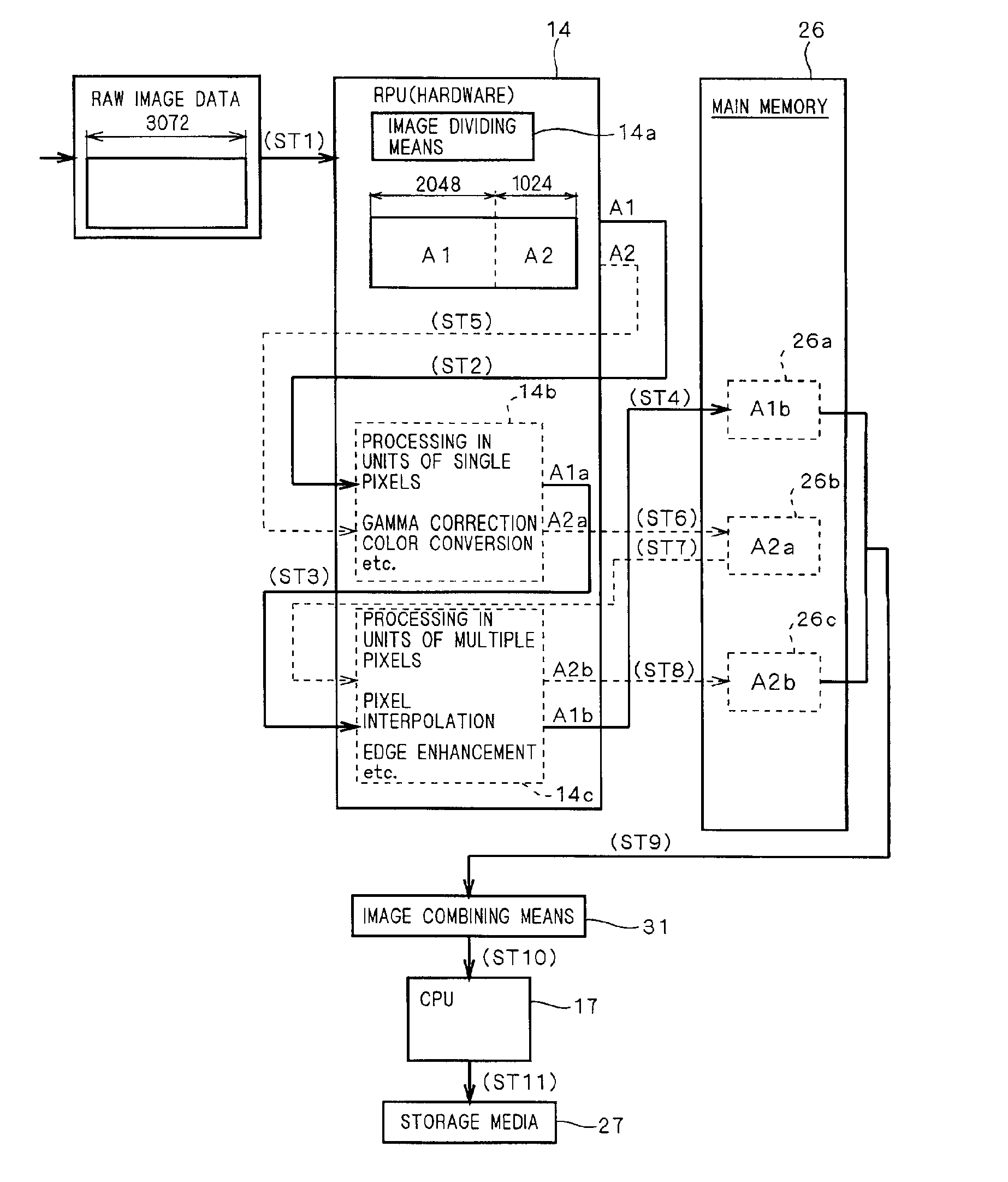
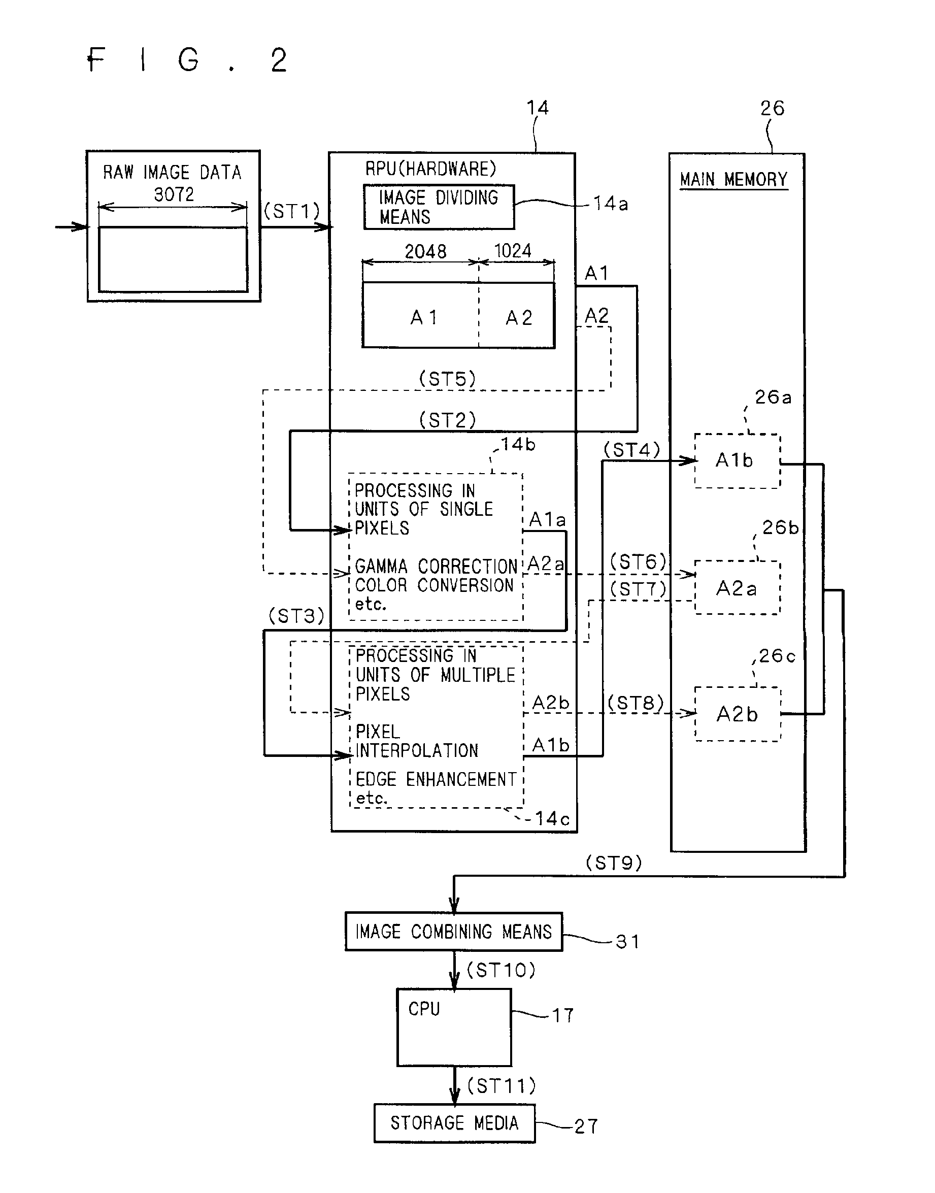
[0042]FIG. 2 is a schematic block diagram for illustrating an image processor according to an embodiment 1 of the present invention. As shown in FIG. 2, the image processor according to the embodiment 1 comprises an RPU (image processing circuit) 14 integrated into a chip, a main memory 26 and image combining means 31. The RPU 14 carries a plurality of line memories (not shown) each having a capacity for 2048 horizontal pixels.

[0043]The RPU 14 comprises image dividing means 14a dividing raw image data having 3072 horizontal pixels input in a progressive system into first divided image data A1 having 2048 horizontal pixels and second divided image data A2 having 1024 horizontal pixels as well as single pixel processing means 14b and multiple pixel processing means 14c image-processing the divided image data A1 and A2 output from the image dividing means 14a in units of single pixels and in units of multiple pixels respectively.

[0044]Examples of the image processing in units of ...

embodiment 2

[0051]

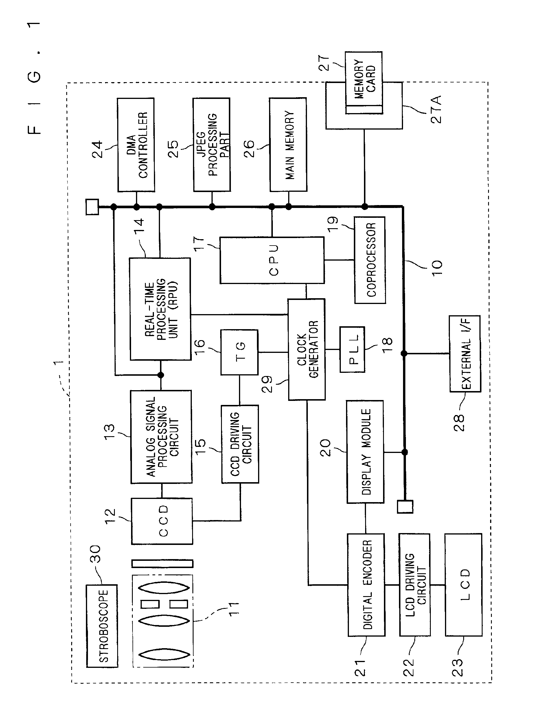
[0052]In order to reduce the load on the CPU 17 and improve the image processing speed, it is preferable to employ the aforementioned DMA controller 24 for data transfer between the RPU 14 and the main memory 26. FIG. 3 is a schematic block diagram for illustrating an image processor according to an embodiment 2 of the present invention employing a DMA controller 24. Referring to FIG. 3, blocks denoted by the same reference numerals as those in FIG. 2 are assumed to have functions similar to the above, and redundant description is omitted. This also applies to step numbers shown in FIG. 3.

[0053]FIG. 4 is a block diagram schematically showing the structure of the DMA controller 24. This DMA controller 24 comprises an arbiter (arbitration circuit) 32, a memory control circuit MC1 and two DMA channels CH0 and CH1. The arbiter 32 and the memory control circuit MC1 are connected to a main bus 10. DMA transfer processing by this DMA controller 24 is as follows: When receiving a DMA ...

embodiment 3

[0058]

[0059]An embodiment 3 of the present invention is now described. FIG. 5 is a schematic block diagram for illustrating an image processor according to the embodiment 3. Referring to FIG. 5, blocks denoted by the same reference numerals as those in FIG. 3 are assumed to have functions similar to the above, and redundant description is omitted. This also applies to step numbers shown in FIG. 5.

[0060]The feature of the embodiment 3 resides in that a circuit structure shown in FIG. 6 is employed for each of DMA channels CH0 and CH1 of a DMA controller 24. A DMA channel CHn (n: 0 or 1) shown in FIG. 6 comprises a register SREG1 storing a transfer start address as in a buffer area of a main memory 26 and another register ERGE1 storing a transfer end address Ae in the buffer area. The transfer start address As and the transfer end address Ae are transferred from a CPU 17 and stored in each register.

[0061]The DMA channel CHn also comprises an address counter AC1 generating / outputting a...


PUM


Abstract

Image dividing means of an RPU divides raw image data into divided image data A1 having 2048 horizontal pixels and A2 having 1024 horizontal pixels. The divided image data A1 is continuously processed in single pixel processing means and multiple pixel processing means and thereafter transferred to and stored in a buffer. The divided image data A2 is processed in the single pixel processing means and thereafter transferred to and temporarily stored in another buffer. The multiple pixel processing means reads and processes divided image data A2a stored in this buffer and thereafter transfers and stores the same to and in still another buffer. Image combining means reads divided image data A1b and A2b stored in the buffers and combines the same with each other. Thus, an image processing time and a cost can be reduced even if raw image data having horizontal pixels in a number exceeding the capacity of a line memory is received.

Description

BACKGROUND OF THE INVENTION[0001]1. Field of the Invention[0002]The present invention relates to an image processor loaded on a digital camera or the like.[0003]2. Description of the Background Art[0004]FIG. 10 is a schematic block diagram of a general digital still camera 100. In the digital still camera 100, an analog image signal picked up with an image pickup sensor 105 such as a CCD sensor or a CMOS sensor is converted to a digital signal and thereafter subjected to various image processing such as gamma correction, color space conversion, pixel interpolation and edge enhancement in an image processing part 106, as shown in FIG. 10. Image data subjected to such image processing is finder-displayed on a liquid crystal monitor 109, compression-coded in the JPEG (joint photographic experts group) system or the TIFF (tag image file format) and stored in a storage medium (memory card) 110 formed by a nonvolatile memory or the like, or output to an external device such as a personal ...

Claims


Application Information

Patent Timeline
IPC IPC(8): G06T1/00H04N5/335G06T3/00G06T1/60H04N1/21H04N1/387H04N5/232H04N101/00
CPCG06T1/0007H04N5/335H04N25/00
Inventor MORIMOTO, KAZUYAMATSUTANI, TAKASHISASAKI, GEN
Owner MEGACHIPS
Why Eureka
Try Eureka