Electrode for an electronic device

a technology of electronic devices and electrodes, applied in the direction of basic electric elements, semiconductor devices, electrical apparatus, etc., can solve the problems of low work function metals, low work function calcium cathode, and only a short time in air

Inactive Publication Date: 2005-09-20
DOLYA HOLDCO 5 LTD
View PDF7 Cites 41 Cited by
  • Summary
  • Abstract
  • Description
  • Claims
  • Application Information

AI Technical Summary

Problems solved by technology

One problem with low work function metals is that they readily react with the environment (e.g., oxygen and moisture).
For example, a low work function calcium cathode survives only a short time in air due to rapid device degradation caused by atmospheric moisture and oxygen.
In addition, the electron injecting layer can be difficult to deposit on the semiconductive layer of the electronic device because, for example, some materials have a high melting point.

Method used


Image

  • Electrode for an electronic device
  • Electrode for an electronic device
  • Electrode for an electronic device

Examples


example 1

(OLED with a Prior Art Electron Injection Layer):

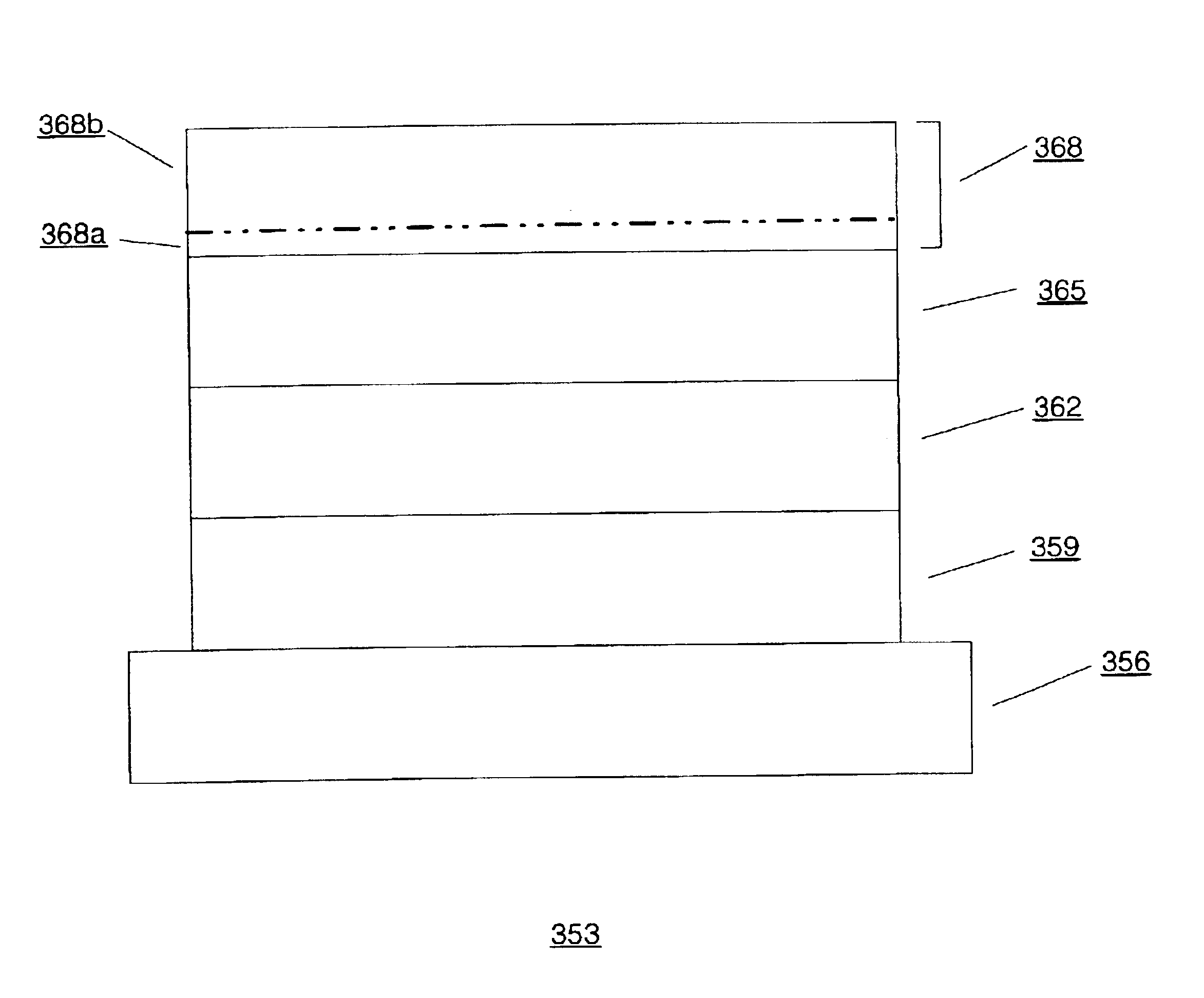
[0069]An OLED was fabricated in the following manner:[0070](1) for the conducting polymer layer, a 70 nm layer of a hole conducting polymer polyethylenedioxythiophene-polystyrenesulfonic acid (“PEDOT:PSS”) was deposited on an anode layer comprised of about 120 nm of indium tin oxide (“ITO”). This conducting polymer is commercially available from H. C. Starck, located in Goslar, Germany[0071](2) for the emissive polymer layer, a 70 nm layer of a substituted polyparaphenylenevinylene was deposited on the 70 nm layer of the conducting polymer layer. The emissive polymer layer is known by its commercial name “Super Yellow” and is commercially available from Covion Organic Semiconductors.[0072](3) for the electron injecting layer, a barium layer was deposited on the emissive layer by resistive-heating in a vacuum evaporator such that the barium layer was evaporated and deposited onto the emissive layer. The thickness of the barium layer is...

example 2

[0074]An OLED was fabricated in the following manner:[0075](1) for the conducting polymer layer, a 70 nm layer of a hole conducting polymer PEDOT:PSS was deposited on an anode layer comprised of about 120 nm of ITO.[0076](2) for the emissive polymer layer, a 70 nm layer of Super Yellow was deposited on the 70 nm layer of PEDOT:PSS.[0077](3) for the electron injecting layer, a cesium oxide layer was deposited on the Super Yellow layer. The thickness of the cesium oxide layer is 0.2 nm. The cesium oxide layer was formed by the resistive heating of the cesium carbonate, Cs2CO3, in a vacuum evaporator resulting in a thermal decomposition of the cesium carbonate. The thermal decomposition of the cesium carbonate produced two compounds: the cesium oxide and the carbon dioxide. The produced cesium oxide was deposited on the emissive layer and the carbon dioxide was removed by the vacuum. The cesium carbonate is commercially available from Aldrich Chemical Company located in Milwaukee, Wis....

example 3

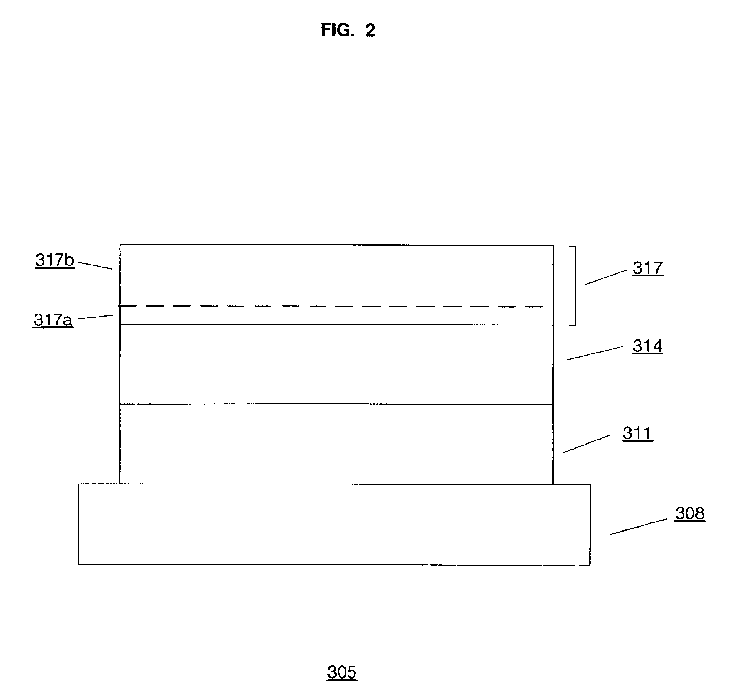
[0082]An OLED was fabricated in the following manner:[0083](1) for the conducting polymer layer, a 70 nm layer of a hole conducting polymer PEDOT:PSS was deposited on an anode layer comprised of about 120 nm of ITO.[0084](2) for the emissive polymer layer, a 70 nm layer of Super Yellow was deposited on the 70 nm layer of PEDOT:PSS.[0085](3) for the electron injecting layer, the cesium oxide layer was deposited on the Super Yellow layer. The cesium oxide layer was formed by the resistive heating of the cesium carbonate, Cs2CO3, in the vacuum evaporator resulting in the thermal decomposition of the cesium carbonate. The thermal decomposition of the cesium carbonate produced two compounds: the cesium oxide and the carbon dioxide. The produced cesium oxide was deposited on the emissive layer and the carbon dioxide was removed by the vacuum.[0086](4) for the conductive cathode layer, a 250 nm layer of aluminum was deposited on the cesium oxide layer.

[0087]One set of OLED displays were pr...


PUM


Abstract

An embodiment of the present invention pertains to an electrode that includes a metal oxide layer, and a conductive layer on that metal oxide layer. The metal oxide layer is an alkali metal oxide or an alkaline earth metal oxide that is formed by: (1) decomposing a compound that includes (a) oxygen and (b) an alkali metal or an alkaline earth metal, or (2) thermally reacting at least two compounds where one of the at least two compounds includes the alkali metal or the alkaline earth metal, and another one of the at least two compounds includes oxygen. The metal oxide layer can also be formed by thermally reacting at least two compounds where one of those compounds includes (a) oxygen and (b) an alkali metal or an alkaline earth metal.

Description

BACKGROUND OF THE INVENTION[0001]Electronic devices need an electrode that provides a low contact resistance with a semiconductive material. Example of electronic devices include organic and inorganic electronic devices. Examples of organic electronic devices include organic light emitting diodes (“OLEDs”) (the OLED can be used in, for example, a display or as a light source element of a light source used for general purpose lighting), organic solar cells, organic transistors, organic detectors, and organic lasers. Such devices typically include a pair of electrodes (e.g., an anode and a cathode) with at least one semiconductive layer between the electrodes.[0002]In the particular case of the OLED, the OLED is typically comprised of two or more thin organic layers (e.g., a conducting polymer layer and an emissive polymer layer where the emissive polymer layer emits light) separating its anode and cathode. Under an applied potential, the anode injects holes into the conducting polyme...

Claims


Application Information

Patent Timeline
Patent Type & Authority Patents(United States)
IPC IPC(8): H01L21/02H01L21/16H01L21/00H01L51/50
CPCH01L51/5092H10K50/171
Inventor STEGAMAT, REZAALLEMAND, PIERRE-MARC
Owner DOLYA HOLDCO 5 LTD
Why Eureka
Try Eureka