Light-emitting element

a technology of light-emitting elements and light-emitting elements, which is applied in the direction of discharge tubes/lamp details, discharge tubes/lamp details, incadescent envelopes/vessels, etc., can solve the problems of low efficiency of extracting light from light-emitting elements, low refractive index of light-emitting layers, and small critical angle, so as to enhance the efficiency of extracting light, increase quantum efficiency, and enhance the effect of extracting ligh

Inactive Publication Date: 2005-09-20
TOYODA GOSEI CO LTD
View PDF29 Cites 42 Cited by
  • Summary
  • Abstract
  • Description
  • Claims
  • Application Information

AI Technical Summary

Benefits of technology

[0088]Concavities and convexities are effective not only in the side surface of the light-emitting area but also in the top surface which is a surface located at the top for extracting light therefrom. For the same reason as in the side surface, that is, because of increase in the net critical angle range, light from the light-emitting area is allowed to emerge from the top surface of the substrate effectively. Since light is allowed to emerge from the side surface and the top surface more effectively, the light-emitting element is designed so that the quantum efficiency further increases.
[0089]In consideration of the above (1) to (26), a light-emitting element according to the present invention has at least a concave or convex surface in the whole surface thereof. The concave or convex surface is employed for enhancing the efficiency of extracting light. The concave or convex surface plays as a role of emitting l...

Problems solved by technology

Thus, there has been a problem that the efficiency of extracting light from the light-emitting element is...

Method used


Image

  • Light-emitting element
  • Light-emitting element
  • Light-emitting element

Examples


embodiment 1

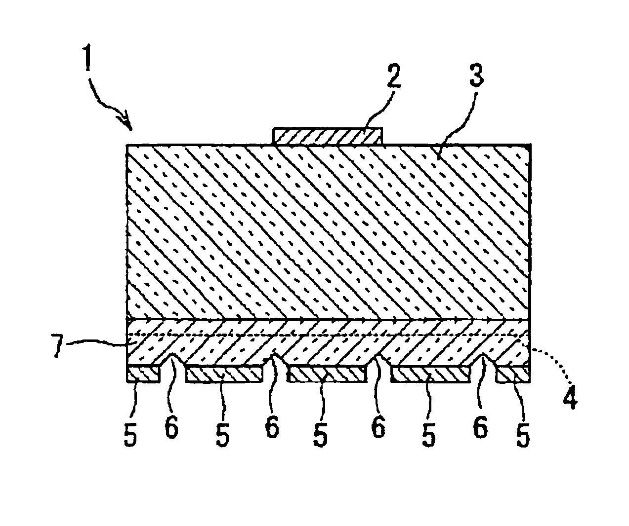
[0115]First, description will be made on Embodiment 1 of the invention with reference to FIGS. 1A to 1C. FIG. 1A is a longitudinal sectional view showing the configuration of a light-emitting element according to Embodiment 1 of the invention; FIG. 1B is a bottom view thereof; and FIG. 1C is a diagram for explaining the positional relationship between reflecting grooves and a light-emitting layer.

[0116]As shown in FIG. 1A, in a light-emitting element 1 according to Embodiment 1, a GaAs-based crystal layer 7 is epitaxially grown on a GaAs substrate 3 (refractive index n=3.0) so that a light-emitting layer 4 is formed. Then, the substrate 3 side is set as the top surface, and the crystal layer 7 side is set as the bottom surface. An electrode 2 with one polarity is provided on a central portion of the substrate 3 while an electrode 5 with the other polarity is provided all over the bottom surface of the crystal layer 7. After that, wedge-like reflecting grooves 6 are formed at regular...

embodiment 2

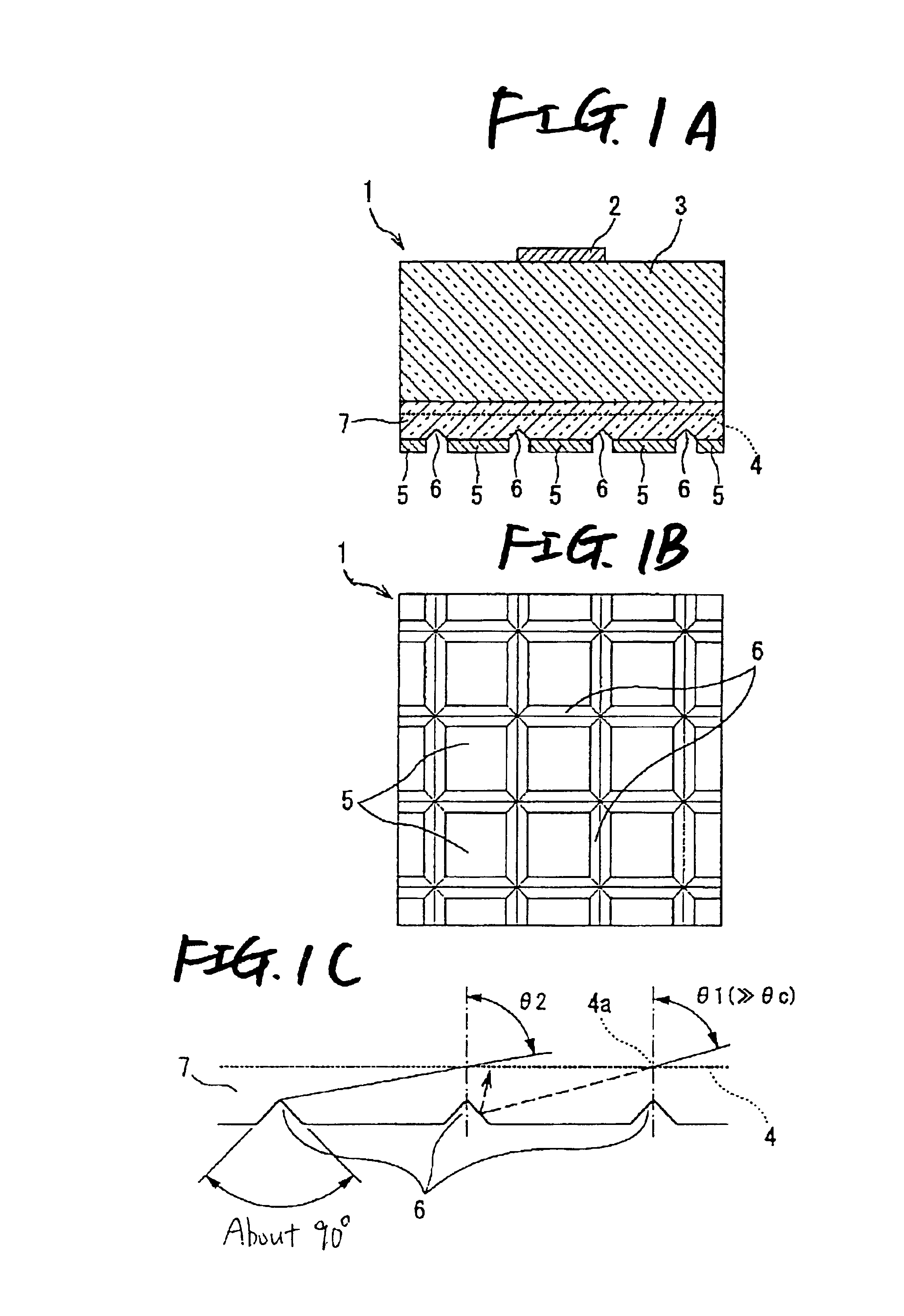
[0119]Next, description will be made on Embodiment 2 of the invention with reference to FIG. 2. FIG. 2 is a longitudinal sectional view showing the configuration of a light-emitting element according to Embodiment 2 of the invention. Incidentally, parts the same as those in Embodiment 1 are referenced correspondingly, and the description of these parts will be omitted.

[0120]As shown in FIG. 2, a light-emitting element 11 according to Embodiment 2 is different from the light-emitting element 1 according to Embodiment 1 in that reflecting grooves 12 are formed to go through the light-emitting layer 4 so as to reach a height above the light-emitting layer 4. As a result, not only light radiated horizontally from each light-emitting point in the light-emitting layer 4 but also light radiated somewhat obliquely upward can be reflected upward by the reflecting grooves 12 formed to go through the light-emitting layer 4. Thus, almost the whole part of the light radiated laterally with a lar...

embodiment 3

[0122]Next, description will be made on Embodiment 3 of the invention with reference to FIGS. 3A and 3B. FIG. 3A is a longitudinally sectional view showing the configuration of a light-emitting element according to Embodiment 3 of the invention, and FIG. 3B is a bottom view thereof. Incidentally, parts the same as those in Embodiments 1 and 2 are referenced correspondingly, and the description of these parts will be omitted.

[0123]As shown in FIGS. 3A and 3B, a light-emitting element 21 according to Embodiment 3 is different from the light-emitting elements 1 and 11 according to Embodiments 1 and 2 in that the light-emitting area of a light-emitting layer 14 is formed as split light-emitting areas formed in places except the places where the reflecting grooves 12 are formed. Then, the reflecting grooves 12 are formed to go through the portions where the light-emitting layer 14 is not formed in the crystal layer 13, so as to reach the height above the light-emitting layer 14. As a res...


PUM


Abstract

A light-emitting element has a light-emitting layer and at lease one light-extracting portion. At least a partial part of the light-extracting portion is formed into a concave or convex surface for enhancing the efficiency of extracting light. Another light-emitting element has a light-emitting layer and a concave or convex surface for reflecting light emitted from the light-emitting layer toward one or more other surfaces of the light-emitting element through an inside of the light-emitting element.

Description

[0001]The present application is based on Japanese Patent Applications No. 2001-159991, 2001-206357 and 2001-304033, which are incorporated herein by reference.BACKGROUND OF THE INVENTION[0002]1. Field of the Invention[0003]The present invention relates to an LED chip (hereinafter referred to as “light-emitting element”) in which a light-emitting layer is formed on a substrate, and light is emitted from the light-emitting layer in response to a voltage applied thereto.[0004]2. Description of the Related Art[0005]In a light-emitting element, for example, a GaAs-based crystal layer or the like is epitaxially grown on a GaAs crystal substrate or the like so that a light-emitting layer is formed. When electrodes of an anode and a cathode are provided and a voltage is applied therebetween, light is emitted from the light-emitting layer, and the light is radiated from the top surface (light-emitting surface).[0006]However, in a light-emitting element, a crystal layer including a light-emi...

Claims


Application Information

Patent Timeline
IPC IPC(8): H01L33/00H01L33/08H01L33/20H01L33/22H01L33/24H01L33/32H01L33/38
CPCH01L33/08H01L33/20H01L33/22H01L33/24H01L33/32H01L33/38
Inventor SUEHIRO, YOSHINOBUKOIKE, MASAYOSHIKATO, HIDEAKI
Owner TOYODA GOSEI CO LTD
Why Eureka
Try Eureka