Semiconductor device with impedance control circuit

a technology of impedance control circuit and semiconductor device, which is applied in the direction of logic circuit coupling/interface arrangement, digital storage, instruments, etc., can solve the problems of external noise affecting external noise can affect the output signal of reflection characteristics, and cause impedance mismatches

Inactive Publication Date: 2005-09-20
SAMSUNG ELECTRONICS CO LTD
View PDF4 Cites 47 Cited by
  • Summary
  • Abstract
  • Description
  • Claims
  • Application Information

AI Technical Summary

Benefits of technology

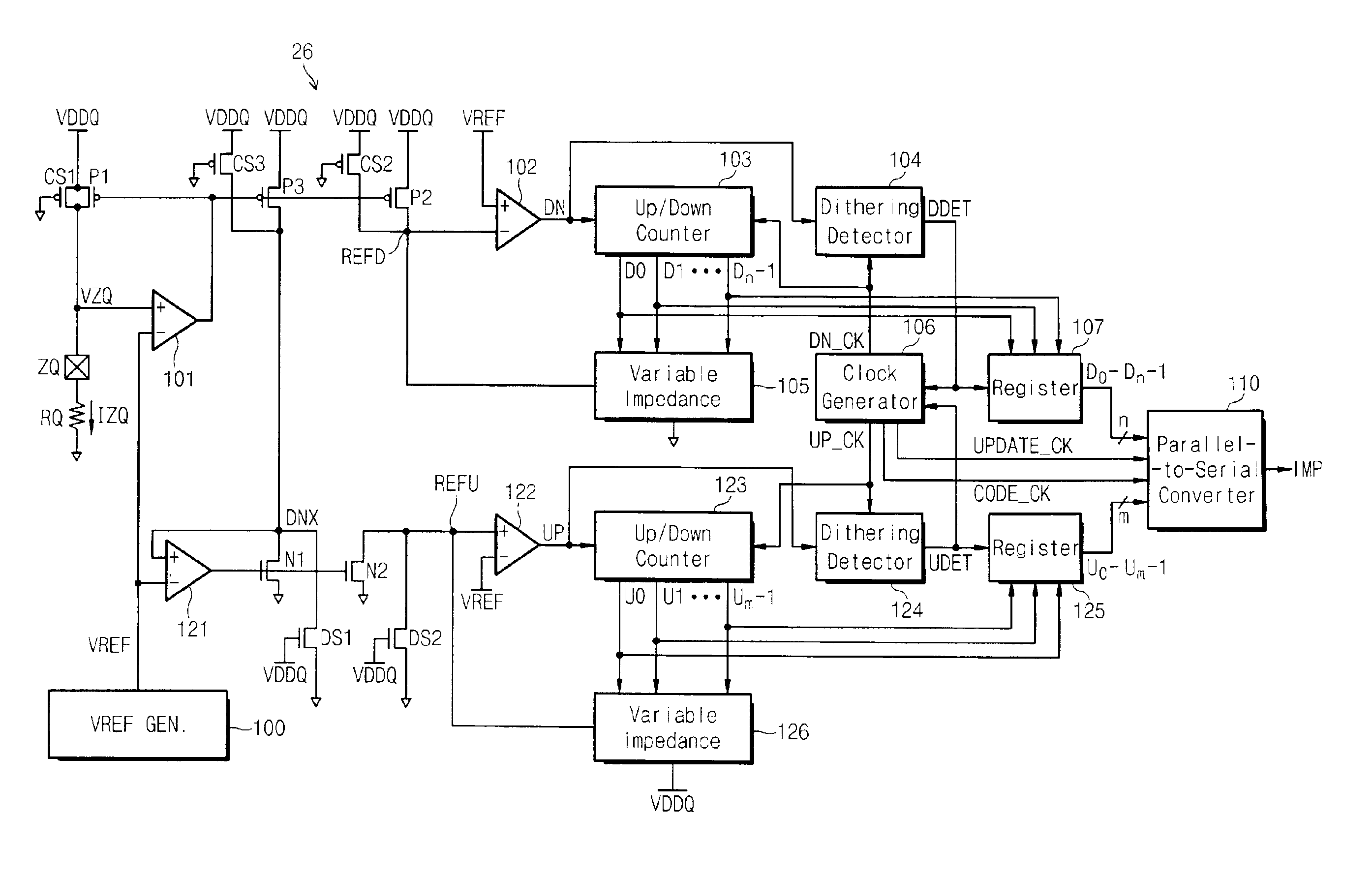
[0014]In the semiconductor device, the output impedance control circuit further comprises a clock generator for generating first to fourth clock signals, the first to third clock signals having the same period and the fourth clock signal having a period shorter than that of the third clock signal.
[0015]In addition, a driving capacity of each of the first to third current source circuits is adjusted by a current controller. In that case, the current controller compares voltages of the

Problems solved by technology

However, as the signal swing width of a transmitted signal decreases, external noise increases.
External noise can affect the reflection characteristics output signal if there is impedance mismatch at an interface.
Impedance mismatch is caused by external noise or by power supply voltage, temperature and process variations.
If impedance mismatch arises, a transmission speed of the data decreases, and the data from a semiconductor device is distorted.
Thus, in a case where a semiconductor device receives distorted data, problems ca

Method used


Image

  • Semiconductor device with impedance control circuit
  • Semiconductor device with impedance control circuit
  • Semiconductor device with impedance control circuit

Examples


Embodiment Construction

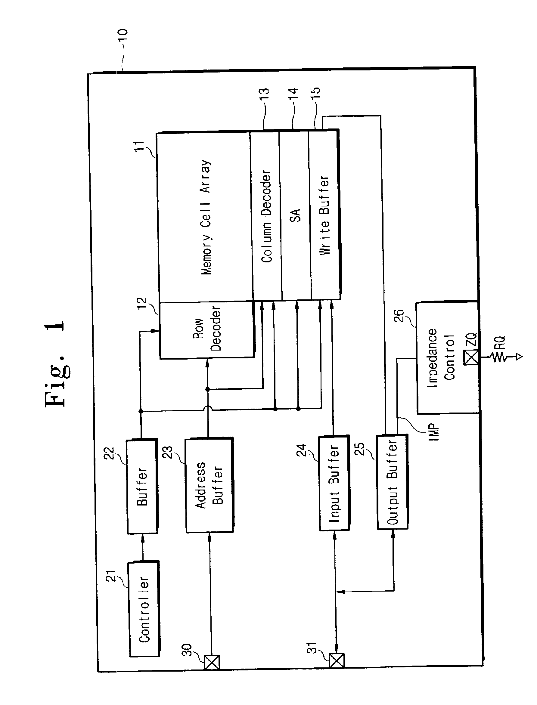
[0034]The preferred embodiment of the invention will be more fully described with reference to the attached drawings.

[0035]FIG. 1 shows a semiconductor device according to the present invention. Referring to FIG. 1, a semiconductor device according to the present invention will be explained using a semiconductor memory device as an example. The semiconductor memory device 10 can be a random access memory such as SRAM or DRAM, or a read only memory such as a FLASH memory or a ferroelectric memory.

[0036]The semiconductor memory device 10 is a memory chip and includes a memory cell array 11, a row decoder circuit 12, a column decoder circuit 13, a sense amplifier circuit 14, a write buffer circuit 15, a read / write control circuit 21, a buffer circuit 22, an address buffer circuit 23, and an input buffer circuit 24, which are well known to those skilled in the art. Thus, a description thereof will be omitted for brevity's sake. The control circuit 21 generates timing control signals for...


PUM


Abstract

A semiconductor device includes an output impedance control circuit, connected to a ZQ pad and an output buffer circuit, for controlling an impedance of the output buffer circuit according to an impedance of an external resistor connected with the ZQ pad.

Description

BACKGROUND OF THE INVENTION[0001]1. Field of the Invention[0002]The present invention relates to semiconductor devices, and more particularly to a semiconductor device that includes an output impedance controller for controlling impedance of an output buffer according to an impedance value of an external resistor.[0003]2. Discussion of Related Art[0004]Many electronic products, for example, personal computers and workstations, include various semiconductor devices such as microcomputers, memories, and gate arrays. The semiconductor devices typically include input / output pins and an output circuit for data transmission with other devices. The output circuit has, for example, output buffers and drivers. The input / output pins of the semiconductor device are connected to corresponding transmission lines such as wires formed on a board. Internal data of a semiconductor device is provided to another semiconductor device through transmission lines that form an interface. For data output fr...

Claims


Application Information

Patent Timeline
IPC IPC(8): G11C7/10H03K19/0175G11C11/401
CPCG11C7/1051G11C7/1057G11C2207/105G11C11/401
Inventor KIM, TAE-HYOUNGCHO, UK-RAEKIM, NAM-SEOG
Owner SAMSUNG ELECTRONICS CO LTD
Why Eureka
Try Eureka