Method for high kinetic energy plasma barrier deposition

Active Publication Date: 2005-09-27
TAIWAN SEMICON MFG CO LTD
View PDF5 Cites 13 Cited by
  • Summary
  • Abstract
  • Description
  • Claims
  • Application Information

AI Technical Summary

Benefits of technology

[0017]In accordance with these and other objects and advantages, the present invention is generally directed to a novel method for depositing a barrier layer on a single damascene, dual damascene or other contact opening structure. The method eliminates the need for pre-cleaning argon ion bombardment of the structure, thereby reducing or eliminating damage to the surface of the underlying conductive layer and sputtering of copper parti

Problems solved by technology

Furthermore, the dual damascene process omits some of the more difficult steps of traditional aluminum metallization, including aluminum etch and many of th

Method used


Image

  • Method for high kinetic energy plasma barrier deposition
  • Method for high kinetic energy plasma barrier deposition
  • Method for high kinetic energy plasma barrier deposition

Examples


Embodiment Construction

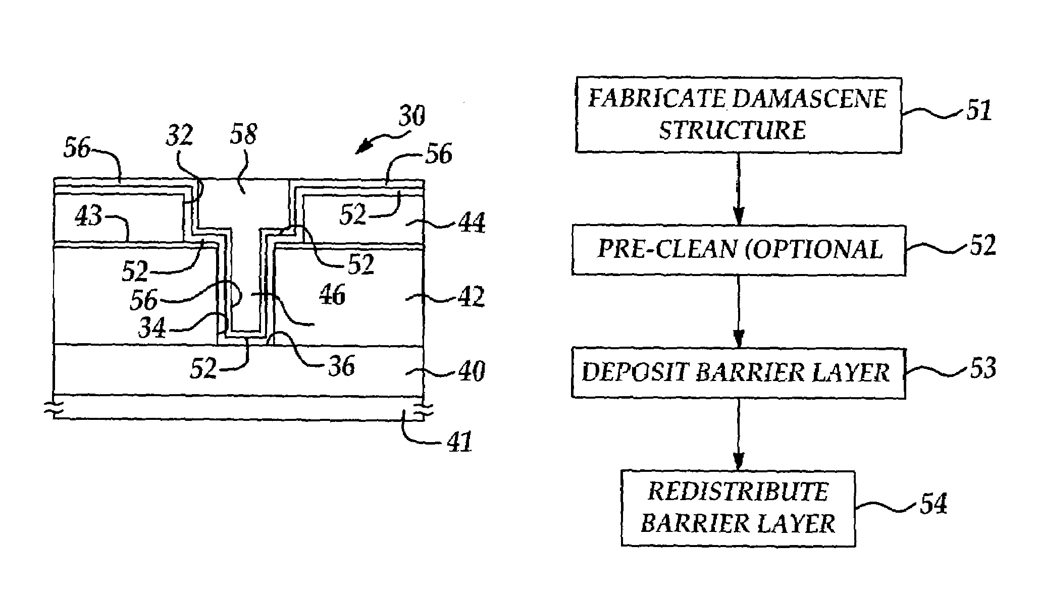
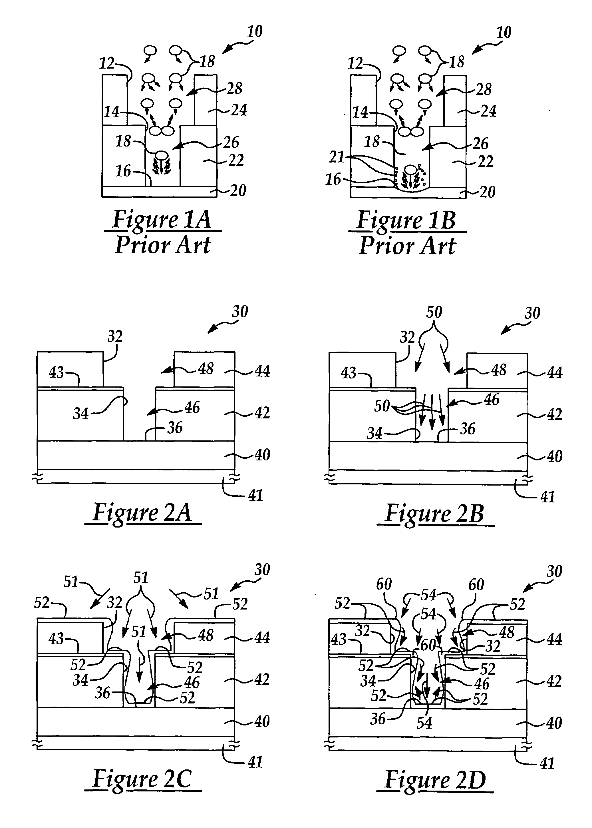
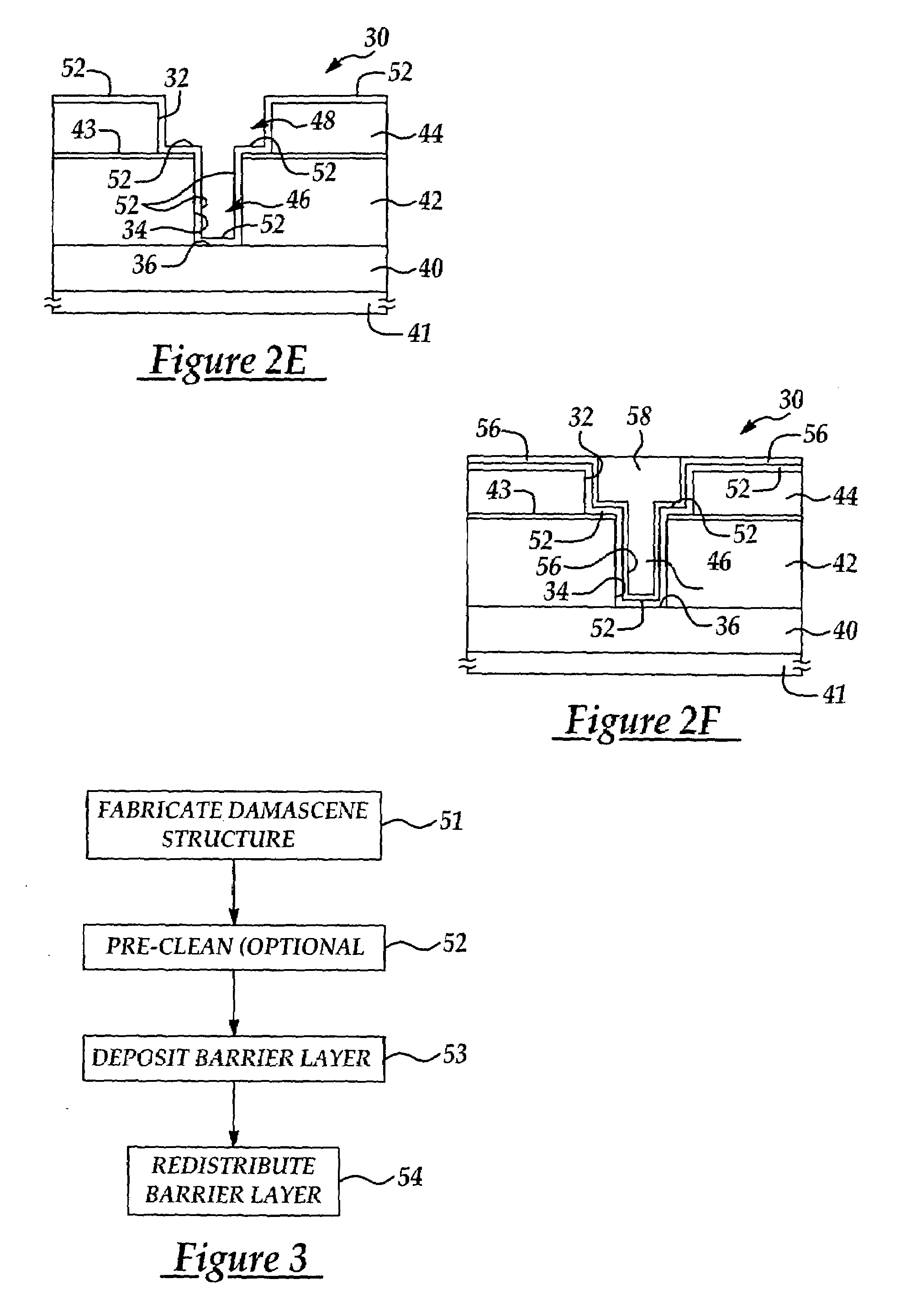
[0029]The present invention has particularly beneficial utility in the deposition of a barrier layer in via and trench openings during the formation of a dual damascene structure on a semiconductor wafer substrate. However, the invention is not so limited in application, and while references may be made to such dual damascene structure, the invention is more generally applicable to deposition of barrier layers in via and trench openings during the formation of single damascene or other contact opening structures during the fabrication of semiconductor integrated circuits.

[0030]Shown throughout FIGS. 2A–3 of the drawings, the present invention is generally directed to a novel method for the deposition of a metal barrier layer on the trench sidewalls, via sidewalls and via bottom of a single damascene, dual damascene or other contact opening structure. The method eliminates the need for barrier pre-deposition argon ion bombardment of those surfaces, thereby reducing or eliminating dam...


PUM


Abstract

A novel method for depositing a barrier layer on a single damascene, dual damascene or other contact opening structure. The method eliminates the need for pre-cleaning argon ion bombardment of the structure, thereby reducing or eliminating damage to the surface of the underlying conductive layer and sputtering of copper particles to the via or other contact opening sidewall. The process includes fabrication of a single damascene, dual damascene or other contact opening structure on a substrate; optionally pre-cleaning the structure typically using nitrogen or hydrogen plasma; depositing a thin metal barrier layer on the sidewalls and bottom of the structure; and redistributing or re-sputtering the barrier layer on the bottom and sidewalls of the structure.

Description

FIELD OF THE INVENTION[0001]The present invention relates to processes for the back-end-of-line (BEOL) cleaning of via sidewalls and bottoms in damascene structures. More particularly, the present invention relates to a novel, high kinetic energy plasma method for the deposition of barrier layers in damascene structures which eliminates the need for argon ion bombardment pre-cleaning (or reactive pre-clean by forming gas (ex:N2 / H2)) of via sidewalls and bottoms.BACKGROUND OF THE INVENTION[0002]The fabrication of various solid state devices requires the use of planar substrates, or semiconductor wafers, on which integrated circuits are fabricated. The final number, or yield, of functional integrated circuits on a wafer at the end of the IC fabrication process is of utmost importance to semiconductor manufacturers, and increasing the yield of circuits on the wafer is the main goal of semiconductor fabrication. After packaging, the circuits on the wafers are tested, wherein non-functio...

Claims


Application Information

Patent Timeline
IPC IPC(8): H01L21/02H01L21/31H01L21/306H01L21/768
CPCH01L21/76843H01L21/76862H01L21/76865H01L21/02046H01L21/2855H01L21/76814
Inventor HUANG, CHENG-LINHSIEH, CHING-HUASHUE, SHAU-LIN
Owner TAIWAN SEMICON MFG CO LTD
Why Eureka
Try Eureka