Image Sensor Having Enhanced Backside Illumination Quantum Efficiency

a backside illumination and image sensor technology, applied in the field of image sensors, can solve the problems of incident light passing through the sensor, degrading the overall performance of pixels of the cmos image sensor, and pixel sensitivity for receiving incident light, so as to increase the quantum efficiency of the backside illumination image sensor, reduce or eliminate damage, and increase the reflectivity of materials

Inactive Publication Date: 2010-04-15
TAIWAN SEMICON MFG CO LTD
View PDF13 Cites 19 Cited by
  • Summary
  • Abstract
  • Description
  • Claims
  • Application Information

AI Technical Summary

Benefits of technology

[0011]These and other problems are generally solved or circumvented, and technical advantages are generally achieved, by embodiments of the present invention which form an image sensor with an enhanced quantum efficiency.
[0015]An advantage of an embodiment of the present invention is an increase in the quantum efficiency of a backside illuminated image sensor due to the increased reflectivity of the materials over the substrate. Additionally, these materials help to reduce or eliminate damage that may occur due to overetching during processing.

Problems solved by technology

Pixel sensitivity for receiving the incident light, however, is lowered with the trend of size reduction of pixels of the CMOS image sensor and cross-talk is caused between different pixels against incident light, especially against incident light with a long wavelength such as the red light (wavelength of about 650 nm), thereby degrading the overall performance of pixels of the CMOS image sensor.
A disadvantage of conventional backside illumination image sensors is that some of the incident light may pass through the sensor and into the overlying dielectric layer.
This may result, however, in defects arising during the manufacturing process. FIG. 1 illustrates two such potential defects, which may arise in a logic area 101 of an integrated circuit in which is formed an image sensor.
However, such an increase in thickness also results in less process control of an etching process used to form contact openings.
Such over-etching can have deleterious effects, such as causing unacceptable levels of leakage current, cross-talk between neighboring devices, and potentially could cause the resulting device to not perform as desired or to not perform at all.
This may cause the etching of the contact opening for contact 111 to overetch the sidewall spacers 116 (shown generally at region 118) and can result in undesired consequences, such as a potential short circuit of the contact 111 to the underlying substrate 100.

Method used


Image

  • Image Sensor Having Enhanced Backside Illumination Quantum Efficiency
  • Image Sensor Having Enhanced Backside Illumination Quantum Efficiency
  • Image Sensor Having Enhanced Backside Illumination Quantum Efficiency

Examples


Embodiment Construction

[0023]The making and using of embodiments of the present invention are discussed in detail below. It should be appreciated, however, that the present invention provides many applicable inventive concepts that can be embodied in a wide variety of specific contexts. The specific embodiments discussed are merely illustrative of specific ways to make and use the invention, and do not limit the scope of the invention.

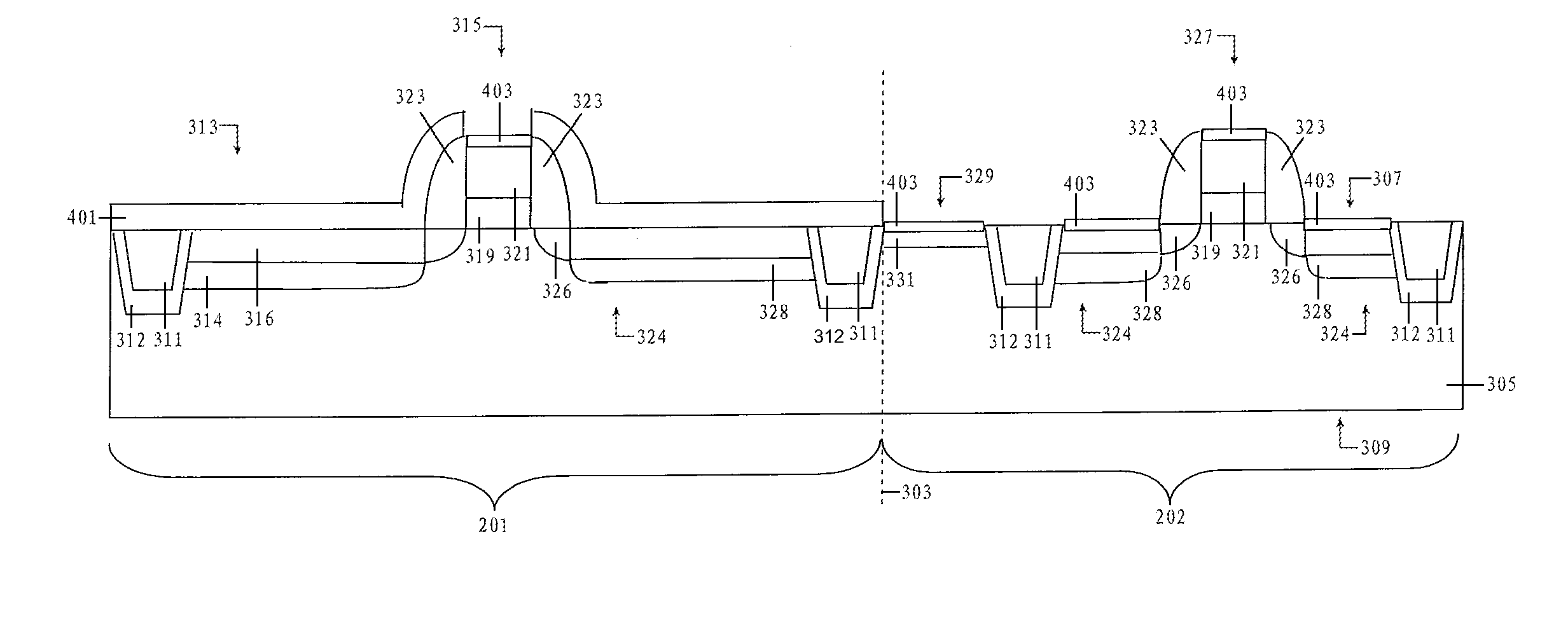
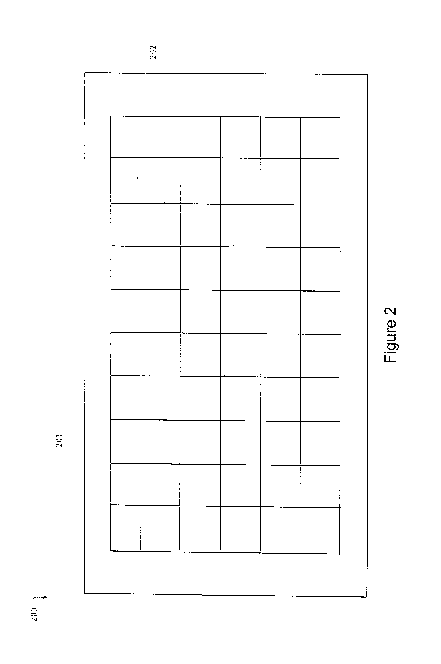
[0024]With reference now to FIG. 2, there is shown an image sensor 200 which comprises a grid or array of backside illuminated pixel regions 201. Each pixel region 201 may comprises a photosensitive diode 313 (not shown in FIG. 2 but illustrated in FIG. 3) which generates a signal related to the intensity or brightness of light that impinges on the photosensitive diode 313.

[0025]The image sensor 200 also may comprise a logic region 202 located adjacent to the array of pixel regions 201. The logic region 202 may have additional circuitry and contacts for input and output conn...


PUM


Abstract

A system and method for image sensing is disclosed. An embodiment comprises a substrate with a pixel region and a logic region. A first resist protect oxide (RPO) is formed over the pixel region, but not over the logic region. Silicide contacts are formed on the top of active devices formed in the pixel region, but not on the surface of the substrate in the pixel region, and silicide contacts are formed both on the top of active devices and on the surface of the substrate in the logic region. A second RPO is formed over the pixel region and the logic region, and a contact etch stop layer is formed over the second RPO. These layers help to reflect light back to the image sensor when light impinges the sensor from the backside of the substrate, and also helps prevent damage that occurs from overetching.

Description

[0001]This application claims the benefit of U.S. Provisional Patent Application Ser. No. 61 / 104,630, filed on Oct. 10, 2008, and entitled “Image Sensor Having Enhanced Backside Illumination Quantum Efficiency,” which application is incorporated herein by reference.TECHNICAL FIELD[0002]The present invention relates generally to an image sensor and a method of manufacturing same and, more particularly, to an image sensor having a dielectric reflector that enhances backside illumination efficiency and a method of manufacturing same that reduces the deleterious effects of over-etching dielectric layers.BACKGROUND[0003]Complementary metal oxide semiconductor (CMOS) image sensors are gaining in popularity over traditional charged-coupled devices (CCDs) due to certain advantages inherent in the CMOS image sensors. In particular, CMOS image sensors typically require lower voltages, consume less power, enable random access to image data, may be fabricated with compatible CMOS processes, and...

Claims


Application Information

Patent Timeline
Patent Type & Authority Applications(United States)
IPC IPC(8): H04N5/335H01L31/0232
CPCH01L27/14603H04N3/155H01L27/1464H01L27/14629H01L21/76829H01L21/76831H01L27/14614H01L27/14621H01L27/14627H01L27/1463H01L27/14636H01L27/14645H01L27/14683H01L27/14685
Inventor LIAO, YIN-KAILIU, HAN-CHILIU, YUAN-HUNGYAUNG, DUN-NIANLIU, JEN-CHENG
Owner TAIWAN SEMICON MFG CO LTD
Why Eureka
Try Eureka