Memory embedded logic integrated circuit mounting memory circuits having different performances on the same chip
a technology of memory circuits and embedded logic, which is applied in the field of memory embedded logic integrated circuit mounting memory circuits having different performance on the same semiconductor chip, can solve the problems of extraordinarily increasing fabrication costs, power consumption cannot be lower than 1 w or less, and expensive packages and heat sinks are required
- Summary
- Abstract
- Description
- Claims
- Application Information
AI Technical Summary
Benefits of technology
Problems solved by technology
Method used
Image

Examples
first embodiment
(First Embodiment)
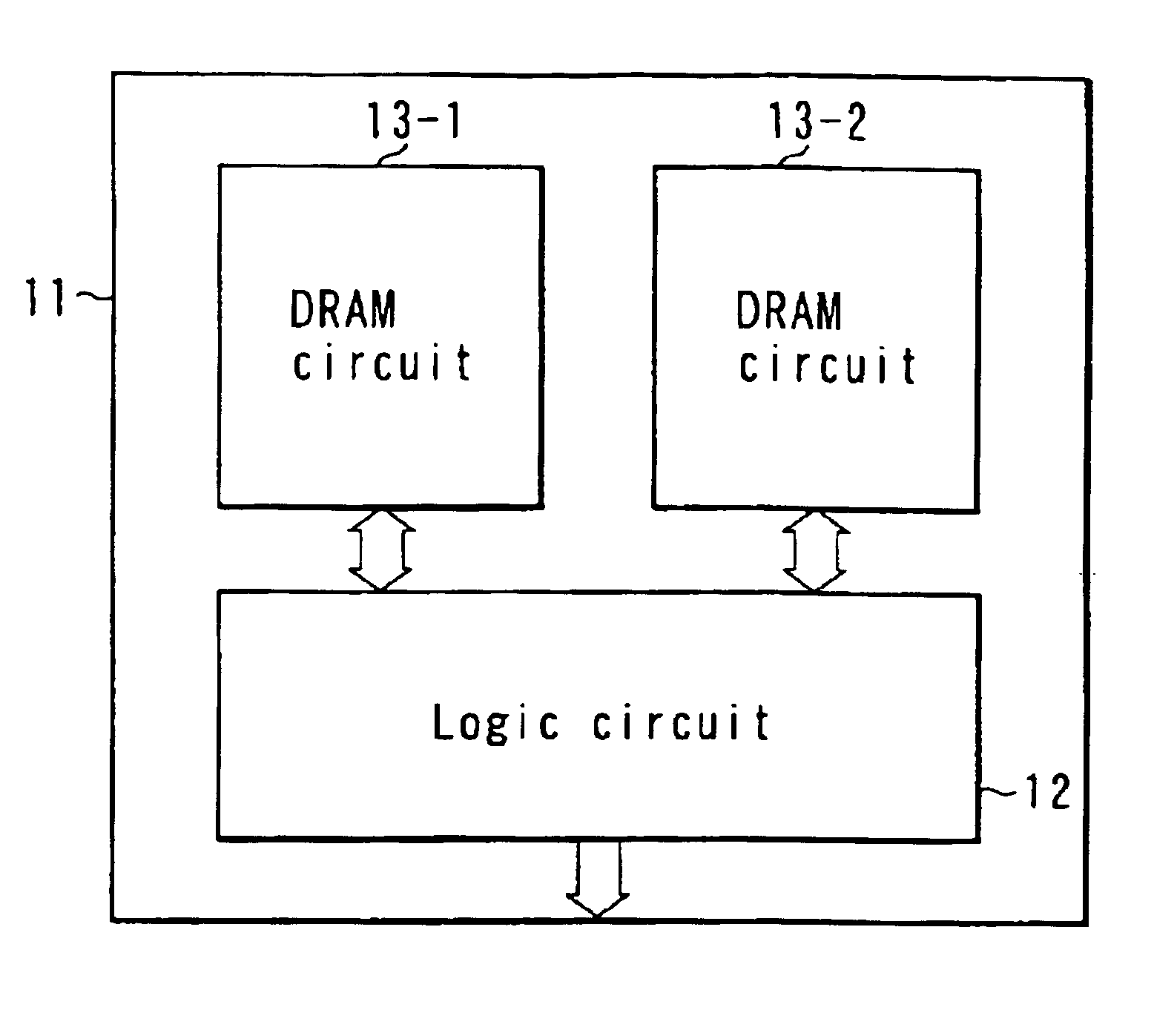
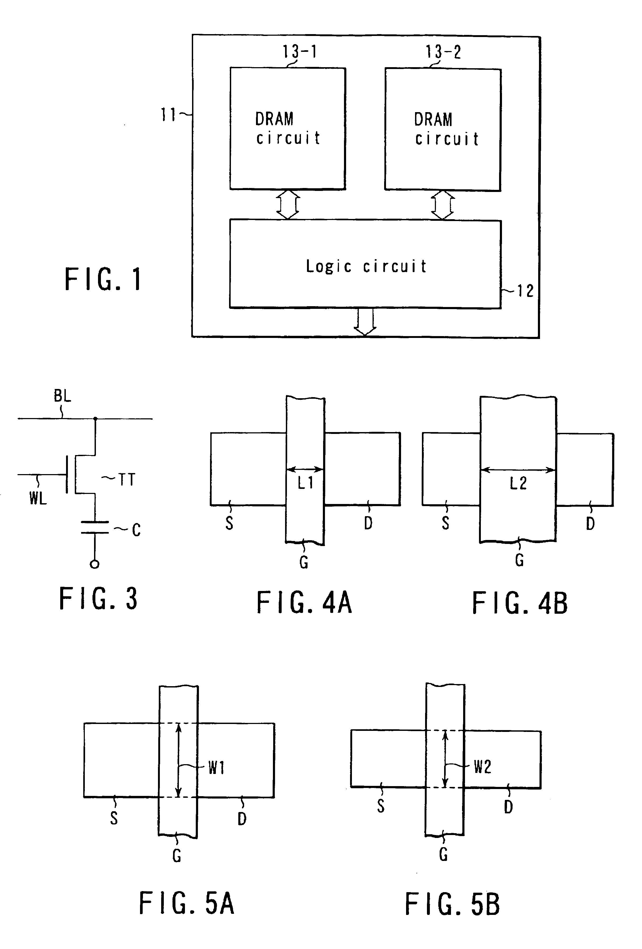
[0042]FIG. 1 shows an outline of the arrangement of a memory embedded logic LSI according to the first embodiment of the present invention. In a semiconductor chip 11, a logic circuit 12 and a plurality of memory circuits 13 are integrated. In this embodiment, first and second DRAM circuits 13-1 and 13-2 are integrated as examples of the memory circuits 13. However, one or more of each of three or more types of DRAM circuits can also be integrated. This similarly applies to each of the following embodiments, so a detailed explanation thereof will be omitted.
[0043]This embodiment will be explained by taking a case in which the first and second DRAM circuits 13-1 and 13-2 are integrated as the memory circuits 13. However, instead of these DRAM circuits, it is also possible to integrate SRAM circuits, nonvolatile memory circuits such as flash memories, ferroelectric memory circuits, or magnetic memory circuits, as the memory circuits 13. This similarly applies to each...
second embodiment
(Second Embodiment)
[0093]In the first embodiment, memory cell arrays in two or more types of DRAM circuits are given different performances by making the values of the ON currents of transfer transistors different from each other.
[0094]However, memory cell arrays in two or more types of DRAM circuits can also be given different performances by making the values of the breaking currents of transfer transistors different from each other. The breaking current herein mentioned is a leakage current which flows when a transistor is OFF.
[0095]Changing the values of the breaking currents of transfer transistors is related to changing the values of the ON currents in the first embodiment; as the ON current value increases, the breaking current value also increases.
[0096]Accordingly, the values of the breaking currents can be changed by using at least one of the means for: changing the channel lengths of transistors as shown in FIGS. 4A and 4B; changing the channel widths of transistors as sh...
third embodiment
(Third Embodiment)
[0100]If the parasitic resistance becomes dominant over the ON resistance of a transfer transistor when memory cell data is to be read out or written, no high-speed operation is possible even if the ON resistance of the transfer transistor is lowered. Therefore, the parasitic resistance is desirably lowered in a DRAM circuit in which a high-speed operation is given high priority. For example, this parasitic resistance is lowered by: lowering the contact resistance by increasing the size of a bit line contact connecting a bit line BL and the drain diffusion layer of a transfer transistor TT shown in FIG. 3; lowering the resistivity of the diffusion layer itself of the transistor TT constructing a memory cell MC; increasing the width of the diffusion layer of the transistor; or lowering the resistive component between the diffusion layer of the transistor constructing the memory cell MC and a capacitor C forming the memory cell.
[0101]FIGS. 8A and 8B are plan views of...
PUM
 Abstract
Description
Claims
Application Information