Integrated circuit with timing adjustment mechanism and method

a timing adjustment and integrated circuit technology, applied in the field of bus systems, can solve the problems of affecting the overall system performance of the system,

Inactive Publication Date: 2005-09-27
RAMBUS INC
View PDF74 Cites 169 Cited by
  • Summary
  • Abstract
  • Description
  • Claims
  • Application Information

AI Technical Summary

Problems solved by technology

However, reduced voltage swings and increasing data rates pose considerable problems to the system designer.
Accordingly, voltage and timing margins for bus signals are often limiting factors in determining overall system performance.
Unfortunately, the ideal voltage and timing margins illustrated in FIG. 2 do not exist in actual bus systems. FIGS. 3A and 3B illustrate typical timing skews between the ideal occurrence of a clock signal within the data eye and actual occurrences.
Such clock timing skews arise from many possible sources, such as differences in the manufacture of signal line traces on printed circuit boards, or differences in signal flight time due to the buildup of standing waves induced by signal and clock reflections and noise on signal lines.
Slight differences in the actual timing of the clock signal and / or the data signal will result in a shift of their ideal timing relationship.
In addition, the bidirectional nature of some signal lines in the bus system will result in timing shifts of different polarities depending on the direction of data flow.
Each one of the multiple slaves connected to the bus might have a different and unpredictable timing error in relation to the ideal clock placement.
Such errors reduce the overall timing margin in the system.
Further, as actual transition times wander, the hazard arises that a device will attempt to read data during a data transition period, i.e., during a period where the data is not valid on the bus.
This hazard increases with system operating frequency.
Such an unequal relationship dramatically reduces the voltage margin for accurately detecting a data value on the bus associated with VHI.
Where the bus system of FIG. 1 uses single-ended data and a single reference voltage, as explained below in greater detail, the presence of voltage errors is particularly harmful.
Unfortunately, a number of system phenomena prevent the stable, centered positioning of VHI and VLO about Vref.
For example, channel-DC resistance induces voltage errors in current mode signaling systems.
In addition, setting output voltage levels to be symmetric about Vref in manufactured systems which experience real process, voltage, and temperature variations is very difficult.
At some point, like the timing errors illustrated above, voltage errors will result in a data error.
However, as bus systems have increased in complexity and size, it has become clear that many factors adversely impacting timing and voltage margins are unique to individual slave devices, or to the relative position of the slave to the master within the overall system.
Thus, the conventional use of timing and voltage offsets in the master has proven ineffective in contemporary bus systems.
Similarly, the use of vernier re-calibration techniques has resulted in inconsistent system performance and unacceptable bandwidth degradation in high frequency systems.

Method used


Image

  • Integrated circuit with timing adjustment mechanism and method
  • Integrated circuit with timing adjustment mechanism and method
  • Integrated circuit with timing adjustment mechanism and method

Examples


Embodiment Construction

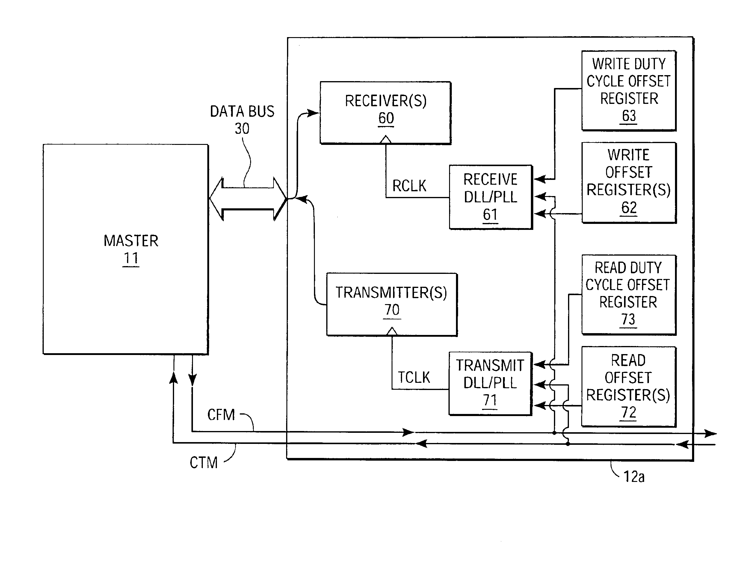
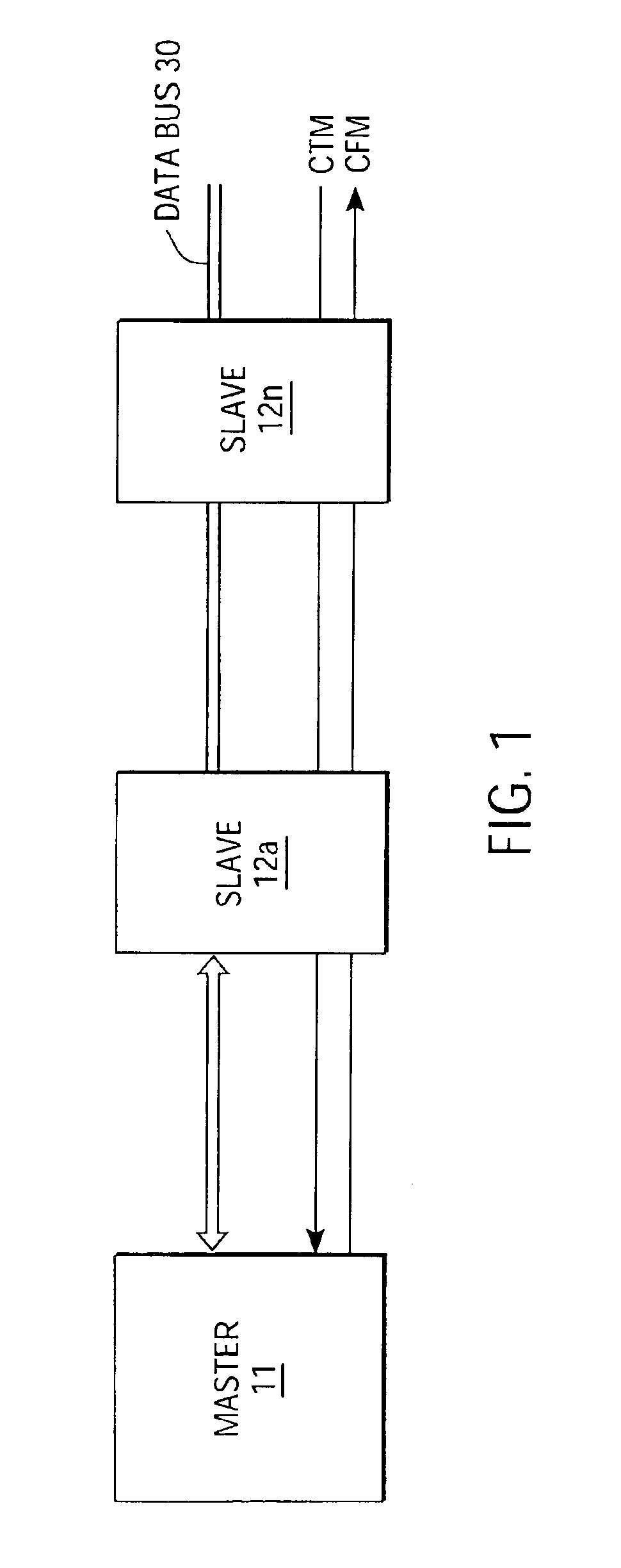
[0063]In order to better understand the use, implementation, and associated benefits of the present invention, a general bus system readily adapted to the present invention will be described with reference to FIG. 5. In the block diagram of FIG. 5, a bus system 10, shown in some additional detail with reference to the bus system shown in FIG. 1, comprises bus 30 coupled between a master 11 and a plurality of slaves 12a-12n. Bus 30 is a high speed, low voltage swing bus comprising multiple signal lines and transferring data between slaves 12a-12n and master 11.

[0064]Master 11 and each slave 12a-12n typically include an interface circuit (not shown) coupling the respective device to bus 30. Within bus system 10, a master can communicate with another master (not shown) and with slaves 12a-12n. In contrast, slaves only communicate with masters.

[0065]Master 11 contains intelligence and generates commands to the slaves. Master 11 may be a microprocessor, a digital signal processor, a grap...


PUM


Abstract

An integrated circuit device includes a receiver, a register and a clock circuit. The receiver samples data from an external signal line in response to an internal clock signal. The register stores a value that represents a timing offset to adjust the time at which the data is sampled. The clock circuit generates the internal clock signal such that the internal clock signal maintains a controlled timing relationship with respect to an external clock signal. The clock circuit includes an interpolator that phase mixes a set of reference clock signals such that the internal clock signal is phase offset in accordance with the value.

Description

[0001]The present invention is a continuation of patent application Ser. No. 09 / 421,073, filed Oct. 19, 1999 now U.S. Pat. No. 6,643,787, which is hereby incorporated by reference.FIELD OF THE INVENTION[0002]The present invention relates to bus systems. More particularly, the present invention relates to a method and apparatus for optimizing the voltage and timing characteristics in a bus system, and to a method for transmitting control information during system calibration.BACKGROUND OF THE INVENTION[0003]Computer systems and other electrical systems typically use one or more buses to interconnect integrated circuits and other system components. Data, typically in digital form, is communicated between such circuits and components via a bus.[0004]Recent trends in bus development have dramatically reduced the voltage swings associated with different data states on the bus. Early bus systems saw rail-to-rail voltage swings from 3.5 or 5.0 volts down to zero volts. More contemporary bu...

Claims


Application Information

Patent Timeline
Patent Type & Authority Patents(United States)
IPC IPC(8): G06F13/42G06F1/10
CPCG06F1/10G06F13/1689G06F13/1694G11C7/1045H04L7/0008G06F13/4243H04L7/033G06F13/364G06F3/061G06F3/0659G06F3/0679G06F12/0246G06F13/404G06F13/4282G06F2212/7201G06F2212/7207
Inventor ZERBE, JARED LEVANDONNELLY, KEVIN S.SIDIROPOULOS, STEFANOSSTARK, DONALD C.HOROWITZ, MARK A.YU, LEUNGVU, ROXANNEKIM, JUNGARLEPP, BRUNO W.HO, TSYR-CHYANGLAU, BENEDICT CHUNG-KWONG
Owner RAMBUS INC
Why Eureka
Try Eureka