Semiconductor device having internal voltage generated stably

a technology of internal voltage and generating circuit, which is applied in semiconductor devices, digital storage, instruments, etc., can solve the problems of increasing the size of the package, increasing the current consumption of the whole system, and increasing the system's scale, so as to achieve a large voltage level change and boost operation

Inactive Publication Date: 2005-10-11
RENESAS ELECTRONICS CORP
View PDF14 Cites 35 Cited by
  • Summary
  • Abstract
  • Description
  • Claims
  • Application Information

AI Technical Summary

Benefits of technology

[0037]By connecting the capacitive elements in parallel to supply electric charges when generating an internal voltage, in the case where an external voltage is high, electric charges can be supplied with sufficient capability, and an internal voltage at a desired voltage level can be stably generated. By changing the voltage level of one of operation pow

Problems solved by technology

In the case of generating the plurality of kinds of voltages externally for application to a DRAM, the scale of a system is increased and, due to loss on external wires, current consumption of the whole system also increases.
In the DRAM as well, since the number of power supply pin terminals increases, the size of the package becomes large.
In a DRAM, in the case where an internal voltage is generated from a

Method used


Image

  • Semiconductor device having internal voltage generated stably
  • Semiconductor device having internal voltage generated stably
  • Semiconductor device having internal voltage generated stably

Examples


first embodiment

[0077]FIG. 1 is a diagram schematically showing the configuration of internal voltage generating circuitry according to a first embodiment of the present invention. The internal voltage generating circuitry shown in FIG. 1 is included in internal voltage generating circuit 900 shown in FIG. 37.

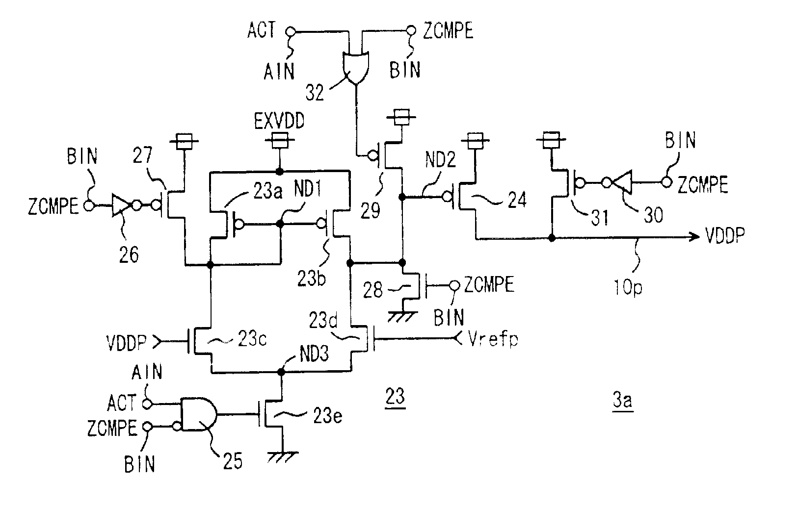
[0078]In FIG. 1, the internal voltage generating circuitry includes; a constant current generating circuit 1 for generating a constant current ICST; an OR circuit 6 receiving an external power supply level designation signal ZCMPE and a power cut enable signal PCUTe; a peripheral reference voltage generating circuit 2p receiving an output signal of OR circuit 6 at a control input DIS and operating, when an output signal of OR circuit 6 is an inactive state (L level), to generate a peripheral reference voltage Vrefp; an array reference voltage generating circuit 2s operating, when power cut enable signal PCUTe supplied to a control input DIS is inactive, to generate an array reference voltage V...

second embodiment

[0140]FIG. 8 is a diagram showing an example of the configuration of an input circuit according to a second embodiment of the present invention. In FIG. 8, in a signal input section for generating an internal signal from an external signal, an input buffer circuit 72 receiving peripheral power supply voltage VDDP as an operation power supply voltage and an input buffer circuit 78 receiving input power supply voltage VDDI as an operation power supply voltage are provided for a common external signal EXSG. In order to selectively enable input buffer circuits 72 and 78, gate circuits 70 and 76 receiving input enable signal EN and mode setting signal MLV are provided.

[0141]Gate circuit 70 enables input buffer circuit 72 when both of input enable signal EN and mode setting signal MLV are at the H level. Gate circuit 76 enables input buffer circuit 78 when input enable signal EN is at the H level and mode setting signal MLV is at the L level.

[0142]Input buffer circuit 72 includes P-channe...

third embodiment

[0163]FIG. 11 is a diagram schematically showing the configuration of internal voltage generating circuitry according to a third embodiment of the present invention. In FIG. 11, peripheral power supply voltage generating circuit 3 is provided to peripheral power supply line 10p, input power supply voltage generating circuit 5 is provided to input power supply line 10i, and array power supply voltage generating circuit 4 is provided to array power supply line 10s. Power cut enable signal PCUTe is supplied to peripheral power supply voltage generating circuit 3, input power supply voltage generating circuit 5 and array power supply voltage generating circuit 4. In the power down mode, array activating signal ACT is in an inactive state. Therefore, when power cut enable signal PCUTe is set to the H level, each of peripheral power supply voltage generating circuit 3, input power supply voltage generating circuit 5 and array power supply voltage generating circuit 4 stops its internal po...


PUM


Abstract

A manner of generating internal voltages such as a high voltage, an intermediate voltage and an internal power supply voltage is switched in accordance with a power supply level setting signal. When the voltage level of an external power supply voltage is low, a current drive transistor receiving an output of a comparing circuit and an auxiliary drive transistor are forcedly set in a conductive state, and external power supply voltage is transmitted on an internal power supply line. At this time, the comparing operation of the comparing circuit is stopped. When the level of the external power supply voltage is high, the comparing circuit is activated down convert the external power supply voltage for generating a peripheral power supply voltage on the internal power supply line.

Description

BACKGROUND OF THE INVENTION[0001]1. Field of the Invention[0002]The present invention relates to a semiconductor device containing an internal voltage generating circuit for generating an internal voltage, and more particularly to an internal voltage generating circuit capable of stably generating an internal voltage in accordance with an external power supply voltage even for specifications of a plurality of external power supply voltages and a plurality of interfaces.[0003]2. Description of the Background Art[0004]FIG. 36 is a diagram schematically showing the configuration of an array portion of a conventional dynamic random access memory (DRAM). In FIG. 36, a memory cell MC is disposed at an intersection of bit lines BL and ZBL and a word line WL. In FIG. 36, memory cell MC disposed at the intersection of the bit line BL and word line WL is representatively shown.[0005]Generally, in a memory array, memory cells MC are disposed in rows and columns, and word line WL is disposed co...

Claims


Application Information

Patent Timeline
IPC IPC(8): G11C11/4074G11C11/407H01L27/04G11C5/14H01L21/822
CPCG11C11/4074G11C5/14
Inventor YAMAUCHI, TADAAKIMATSUMOTO, JUNKOOKAMOTO, TAKEOSUWA, MAKOTOICHIGUCHI, TETSUICHIROYONETANI, HIDEKINAGASAWA, TSUTOMUTIAN, ZENGCHENG
Owner RENESAS ELECTRONICS CORP
Why Eureka
Try Eureka