Resonant cavity III-nitride light emitting devices fabricated by growth substrate removal

a technology of iii-nitride and light-emitting devices, which is applied in the direction of semiconductor devices, laser details, semiconductor lasers, etc., can solve the problems of difficult packaging of geometries and poor fill factor

Active Publication Date: 2005-10-18
LUMILEDS
View PDF13 Cites 97 Cited by
  • Summary
  • Abstract
  • Description
  • Claims
  • Application Information

AI Technical Summary

Problems solved by technology

The device is thus a non-planar surface with narrow insulating blocking layers separating the n- and p-contacts, a geometry that is difficult to package.
Also, much of the area of the active region is lost to the n-contact and insulating regions, providing a poor fill factor.

Method used


Image

  • Resonant cavity III-nitride light emitting devices fabricated by growth substrate removal
  • Resonant cavity III-nitride light emitting devices fabricated by growth substrate removal
  • Resonant cavity III-nitride light emitting devices fabricated by growth substrate removal

Examples


Embodiment Construction

[0024]In accordance with embodiments of the invention, improved III-nitride resonant cavity devices are provided. A constant cavity thickness is created by incorporating an etch stop layer during growth. In some embodiments of the invention, trenches are formed on the device to increase light extraction. In some embodiments, grid contacts are provided.

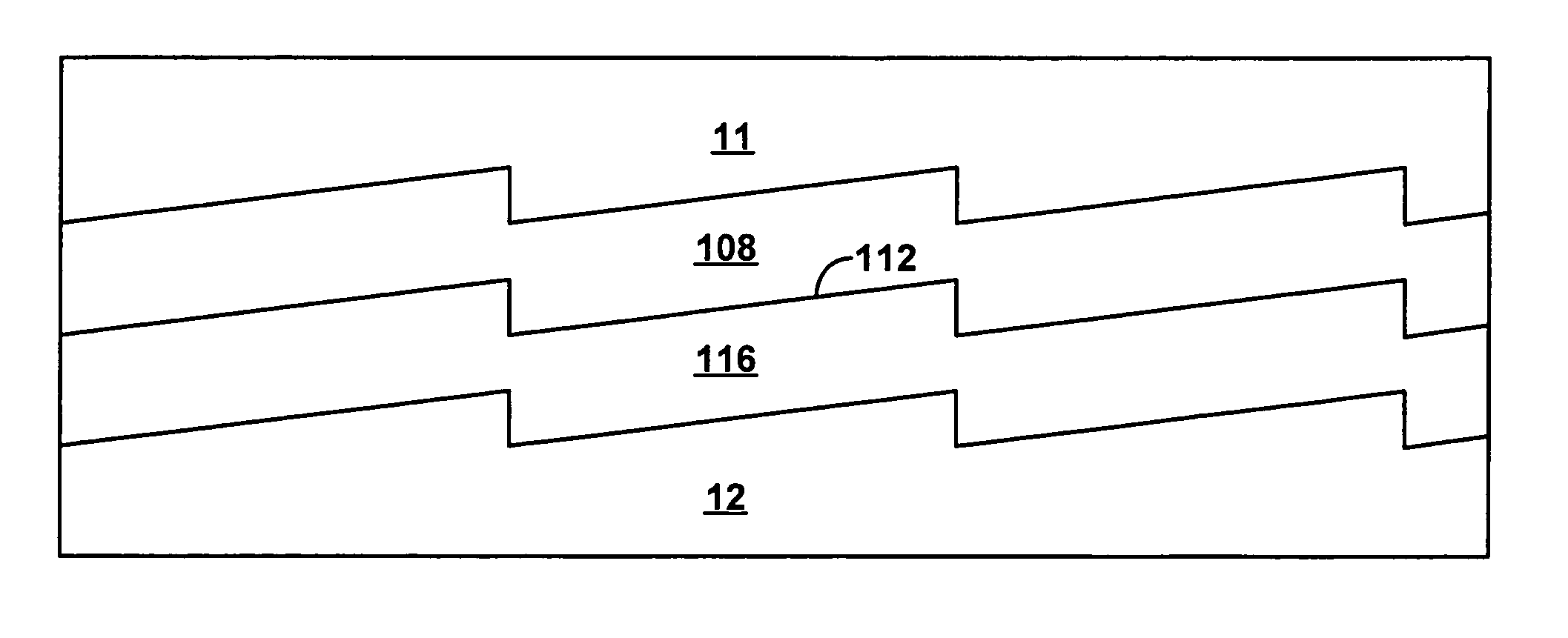
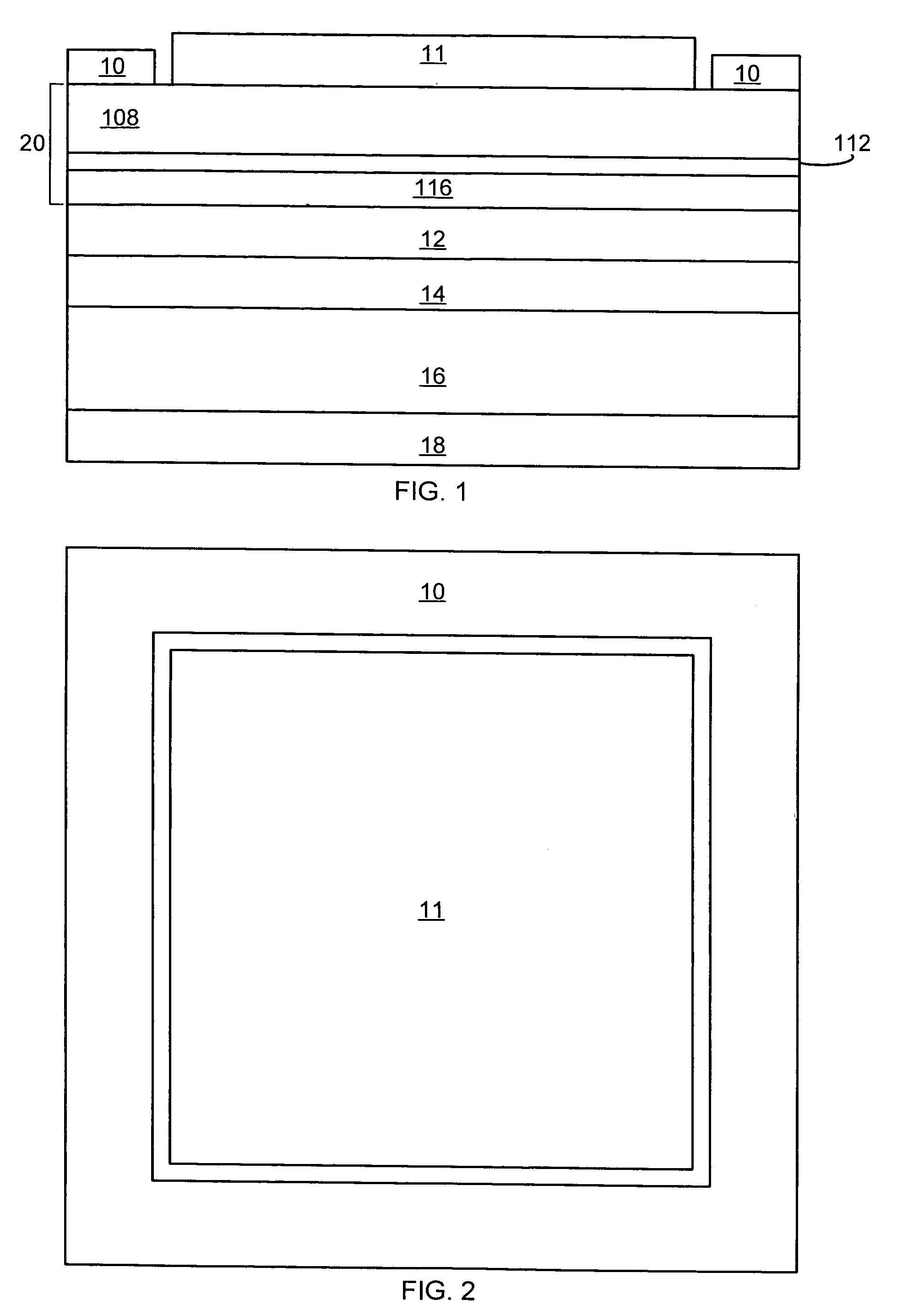
[0025]FIGS. 1 and 2 are cross sectional and plan views of a resonant cavity III-nitride device according to embodiments of the invention. An active region 112 is sandwiched between an n-type region 108 and a p-type region 116. The embodiment of FIGS. 1 and 2 shows an n-contact 10 formed on a portion of n-type region 108 not covered by DBR 11, through which light is extracted from the device. A reflective p-contact 12 is formed on p-type region 116. P-contact 12 connects the epitaxial layers 20 to a host substrate 16 either directly or via optional bonding layers 14. Host substrate 16 may be a semiconductor, requiring ohmic contacts 18 ...


PUM


Abstract

A semiconductor light emitting device includes an n-type region, a p-type region, and light emitting region disposed between the n- and p-type regions. The n-type, p-type, and light emitting regions form a cavity having a top surface and a bottom surface. Both the top surface and the bottom surface of the cavity may have a rough surface. For example, the surface may have a plurality of peaks separated by a plurality of valleys. In some embodiments, the thickness of the cavity is kept constant by incorporating an etch-stop layer into the device, then thinning the layers of the device by a process that terminates on the etch-stop layer.

Description

BACKGROUND[0001]1. Field of Invention[0002]The present invention relates to III-nitride semiconductor light emitting devices.[0003]2. Description of Related Art[0004]Semiconductor light-emitting devices including light emitting diodes (LEDs) are among the most efficient light sources currently available. Materials systems currently of interest in the manufacture of high-brightness light emitting devices capable of operation across the visible spectrum include Group III–V semiconductors, particularly binary, ternary, and quaternary alloys of gallium, aluminum, indium, and nitrogen, also referred to as III-nitride materials. Typically, III-nitride light emitting devices are fabricated by epitaxially growing a stack of semiconductor layers of different compositions and dopant concentrations on a sapphire, silicon carbide, III-nitride, or other suitable substrate by metal-organic chemical vapor deposition (MOCVD), molecular beam epitaxy (MBE), or other epitaxial techniques. Sapphire is ...

Claims


Application Information

Patent Timeline
Patent Type & Authority Patents(United States)
IPC IPC(8): H01L33/00H01S5/183H01L33/46
CPCH01L33/465H01L33/007H01L33/0079H01L33/22H01L33/0093
Inventor EPLER, JOHN E.KRAMES, MICHAEL R.WIERER, JR., JONATHAN J.
Owner LUMILEDS
Why Eureka
Try Eureka