Waveguide to stripline transition with via forming an impedance matching fence

a waveguide and stripline transition technology, applied in the direction of coupling devices, multiple-port networks, electrical devices, etc., can solve the problems of increasing the complexity of the structure, and achieve the effect of facilitating the manufacturing process and being less expensiv

Inactive Publication Date: 2005-10-25
RPX CORP
View PDF6 Cites 134 Cited by
  • Summary
  • Abstract
  • Description
  • Claims
  • Application Information

AI Technical Summary

Benefits of technology

[0008]It is the object of the present invention to improve the known device for guiding electromagnetic waves in a way that the manufacturing process is made easier and less expensive.

Problems solved by technology

The prior art approach for achieving impedance matching is based on a complex structure which can only be realised in a difficult and expensive manufacturing process.
Attaching the back-short further increases the complexity of the structure.

Method used


Image

  • Waveguide to stripline transition with via forming an impedance matching fence
  • Waveguide to stripline transition with via forming an impedance matching fence
  • Waveguide to stripline transition with via forming an impedance matching fence

Examples


first embodiment

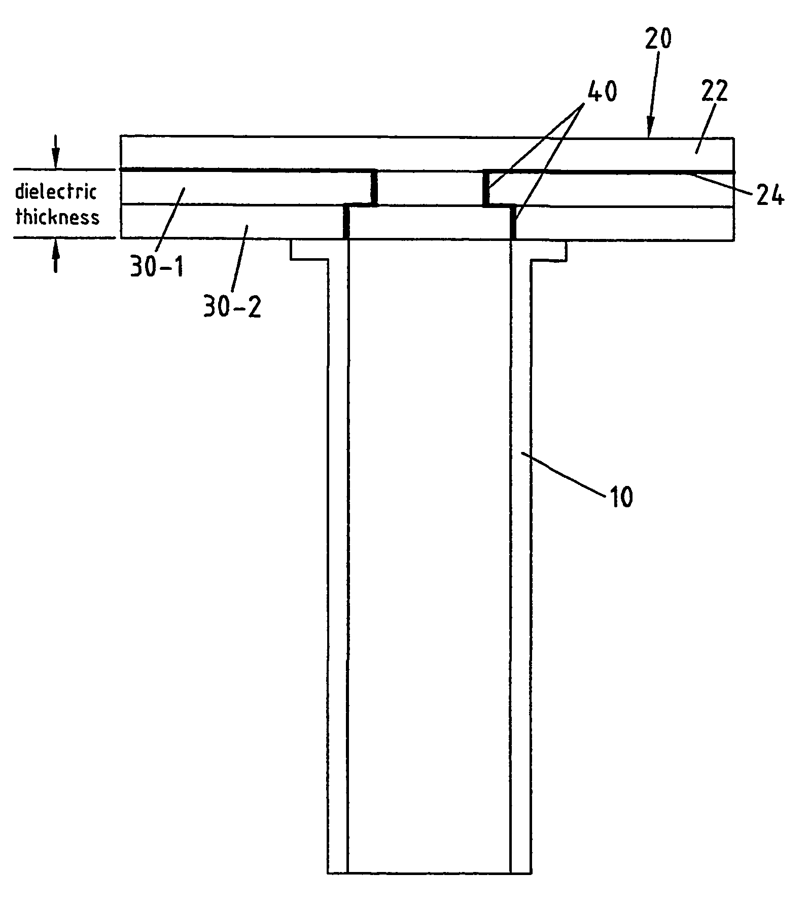
[0027]FIG. 1 shows a structure for guiding electromagnetic waves according to the invention. The structure comprises a wave guide 10 and a transmission line 20, the substrate layer 22 of which is arranged perpendicular to the longitudinal axis of the wave guide 10 for transition of electromagnetic waves from the wave guide 10 to the transmission line 20. There are two layers 30-1 and 30-2 provided as coupling means, the layers 30-1, 30-2 being arranged between the substrate layer 22 of the transmission line 20 and the wave guide 10, wherein the dielectric thickness of the layers 30-1, 30-2 is adjusted in a way described below.

[0028]Each of the layers 30-1, 30-2 comprises metallised through-holes 40, called “vias”, forming a fence-like structure surrounding the area of each layer 30-1, 30-2, respectively, through which the wave should be guided. Vias of different layers are interconnected with each other and with a metallised layer 24 at the bottom side of the substrate layer 22 of t...

second embodiment

[0035]FIG. 5 shows a structure according to the present invention in which three layers, 30-1, 30-2, 30-3, between the substrate 22 of the transmission line 20 and the wave guide 10 comprises vias 40. Quite often it is sufficient to optimise just only the dimensions of the layer 30-1 directly beneath the micro strip ground plane 24 and to keep elsewhere in the substrate the dimensions equal to the cross-sectional area of the metal wave guide 10. In general it appears that the larger the dimensions of the wave guide continuation structure in the dielectric substrate of the layers 30-1, 30-2, 30-3 and the transmission line 20, the smaller the insertion loss.

[0036]According to the present invention the preferred material for the dielectrical layers is low or high temperature co-fired ceramic LTCC or HTCC.

[0037]The process for manufacturing said layers comprising vias is illustrated in FIG. 6. In a first step S1, the substrate is generated by mixing solvents, ceramic powder and plastic ...

third embodiment

[0038]FIG. 7 shows a third embodiment for a structure for guiding electromagnetic waves according to the present invention. It substantially corresponds to the structure shown in FIG. 5 however, the implementation of the vias in the layers is shown in more detail and layers 30-4, 30-5, 30-6, and 30-7 are additionally comprised within the structure.

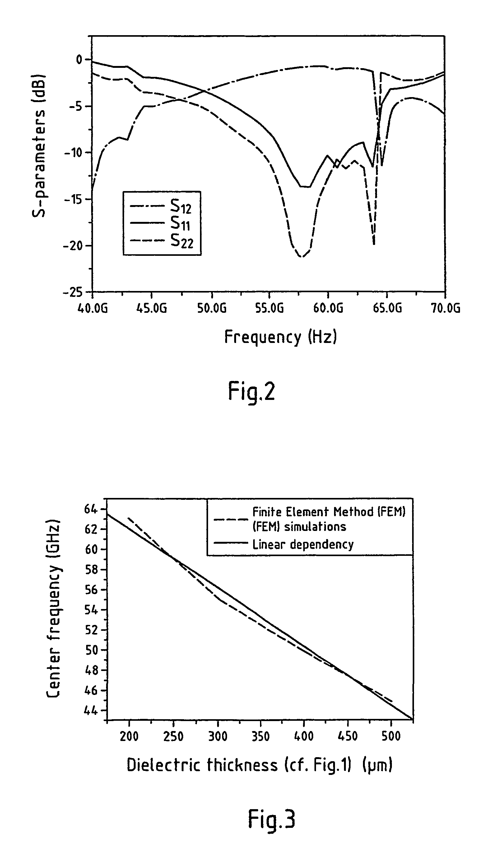
[0039]Whereas in FIG. 5 all layers 30-1, . . . 30-3 have the same thickness, the thickness of layer 30-2 in FIG. 7 has been varied in order to achieve good impedance matching. For example, for achieving good impedance matching at a particular frequency of 60 GHz it has been found that the appropriate thickness of layers 30-1 and 30-4 to 30-7 shall be 100 μm, whereas the thickness of layer 30-2 is proposed to be 150 μm.

[0040]The vias in the dielectric substrate layers do not only influence the impedance matching but also have an important roll in the mechanical design of the structure because they preferably connect the ground planes 24, 31...


PUM


Abstract

The invention relates to a device for guiding electromagnetic waves from a wave guide (10), in particular a multi-band wave guide, to a transmission line (20), in particular a micro strip line, arranged at one end of the wave guide (10), comprising coupling means (30-1, . . . , 30-7) for mechanical fixation and impedance matching between the wave guide (10) and the transmission line (20). It is the object of the invention to improve such a structure in the way that manufacturing is made easier and less expensive than according to prior art. According to the present invention that object is solved in the way that the coupling means comprises at least one dielectric layer (30) being mechanically connected with the main plane of the transmission line, the geometric dimension of that at least one dielectric layer extending along the propagation direction of the electromagnetic waves being correlated with the center frequency of electromagnetic waves in order to achieve optimised impedance matching.

Description

BACKGROUND OF THE INVENTION[0001]1. Field of the Invention[0002]The invention relates to a device for guiding electromagnetic waves from a wave guide, in particular a multi-band wave guide, to a transmission line, in particular a microstrip line, arranged at one end of the wave guide, comprising coupling means for mechanical fixation and impedance matching between the wave guide and the transmission line.[0003]One problem for devices of that kind is to ensure a good transmission of electrical power in the wave guide to transmission line transition. Poor transition results in large insertion loss and this may degrade the performance of the whole module, e.g. a transceiver module.[0004]2. Description of the Related Art[0005]A device with a structure known in the prior art is shown in FIG. 9. There is shown a wave guide 10 and a transmission line 20, in particular a micro strip structure which are attached to each other for enabling transition of electromagnetic waves from the wave gui...

Claims


Application Information

Patent Timeline
Patent Type & Authority Patents(United States)
IPC IPC(8): H01P5/107H01P5/10
CPCH01P5/107
Inventor SALMELA, OLLIKOIVISTO, MARKKUSAARIKOSKI, MIKKOJOKIO, KALLEARSLAN, ALI NADIRKEMPPINEN, ESAKORHONEN, VESAMIETTINEN, TEPPO
Owner RPX CORP
Why Eureka
Try Eureka