Method of fabricating three dimensional gate structure using oxygen diffusion

a three-dimensional gate structure and oxygen diffusion technology, applied in the direction of semiconductor devices, electrical appliances, transistors, etc., can solve the problems of increasing the difficulty of maintaining high performance characteristics, becoming increasingly difficult to fabricate the needed smaller dimensions of mosfet features, and forming thin fin structures (approximately 20 nm in width) from a soi (semiconductor on insulator) structure,

Active Publication Date: 2005-11-01
NORTH STAR INNOVATIONS
View PDF8 Cites 28 Cited by
  • Summary
  • Abstract
  • Description
  • Claims
  • Application Information

AI Technical Summary

Problems solved by technology

As the MOSFET device is further miniaturized, however, it becomes increasingly difficult to maintain high performance characteristics.
It also becomes increasingly technically challenging to fabricate the MOSFET features in the needed smaller dimensions.
Previously the formation of thin fin structures (approximately 20 nm in width) from an SOI (semiconductor on insulator) structure has been problematic.
These other techniques, generally involving forming a larger silicon structure than desired for the final size, and then trimming the structure dimension through various means to the desired measure, have drawbacks that render them unacceptable.
This method, however, is limited by manufacturing considerations to creating fins that are not less than approximately 30 nm in width.
Thus, the technique is not viable for technology nodes going below that dimension.
RIE is also an undesirable technique in that it generates fin structures with surface roughness.
Surface roughness leads to poor electrical performance in the finished transistor.
Further, RIE methods have poor dimensional control in the wafer method of manufacture; this drawback results in nonuniformity between transistors at different points on a wafer.
Thus, RIE is an undesirable method of manufacturing.
However, there is an inherent drawback to this process that renders this method undesirable.
The process promotes weakness at the point where the silicon fin meets the silicon dioxide substrate layer, the base portion of the fin.
Necking results in a mechanical weakening of the fin; and this weakness leads to problems during the subsequent processing steps that take place in industrial fabrication methods.
Further, the narrowing of the fin affects the electrical characteristics of the fin.
Hence a pure oxidation is an unattractive method for shaping a fin to a desired dimension.

Method used


Image

  • Method of fabricating three dimensional gate structure using oxygen diffusion
  • Method of fabricating three dimensional gate structure using oxygen diffusion
  • Method of fabricating three dimensional gate structure using oxygen diffusion

Examples


Embodiment Construction

[0017]The following detailed description of the invention is merely exemplary in nature and is not intended to limit the invention or the application and uses of the invention. Furthermore, there is no intention to be bound by any theory presented in the preceding background of the invention or the following detailed description of the invention.

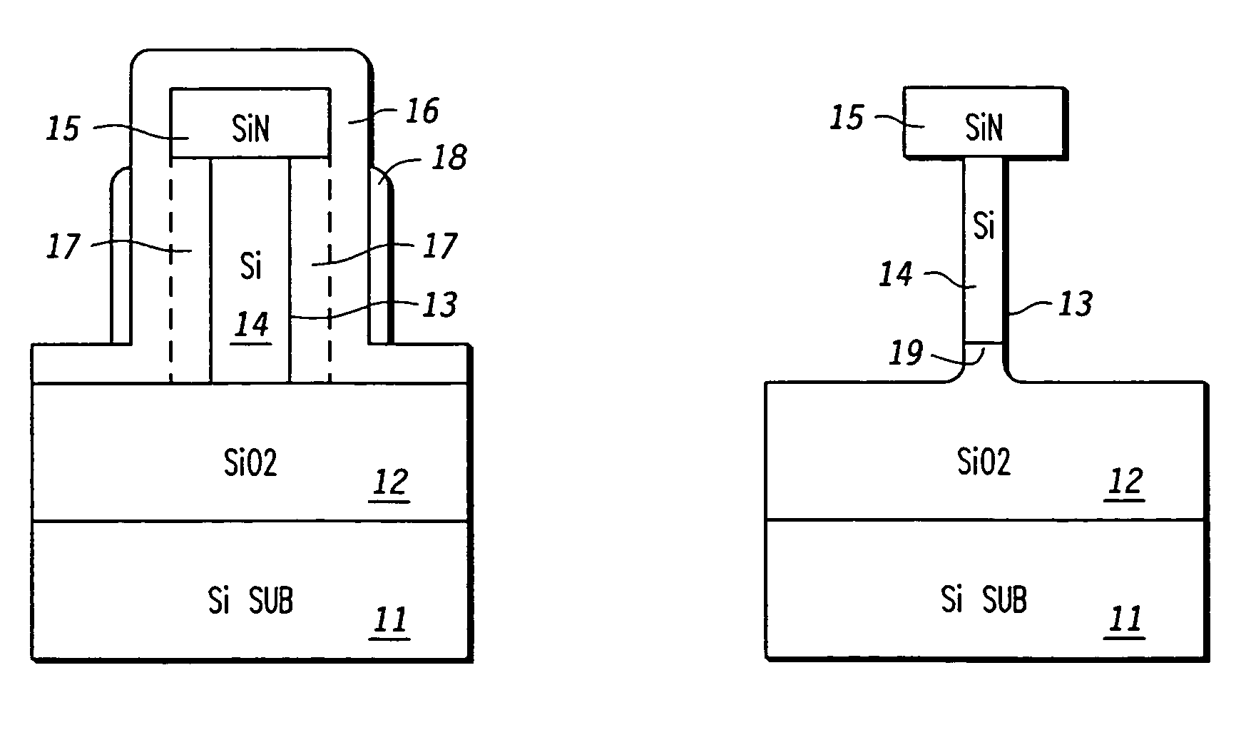
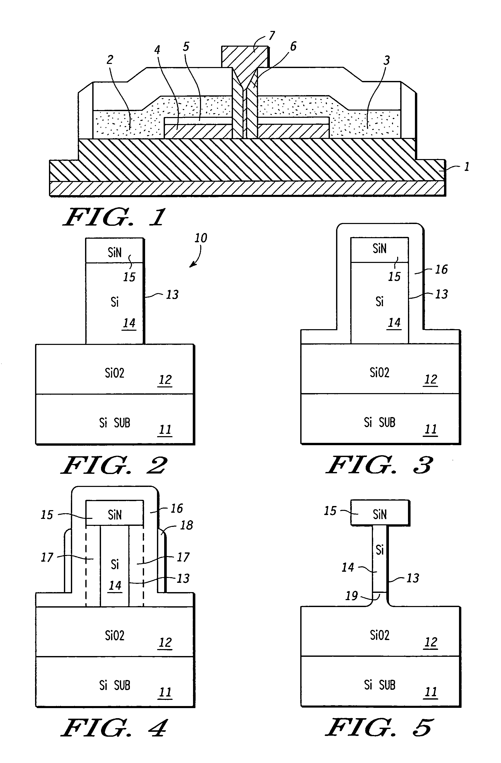
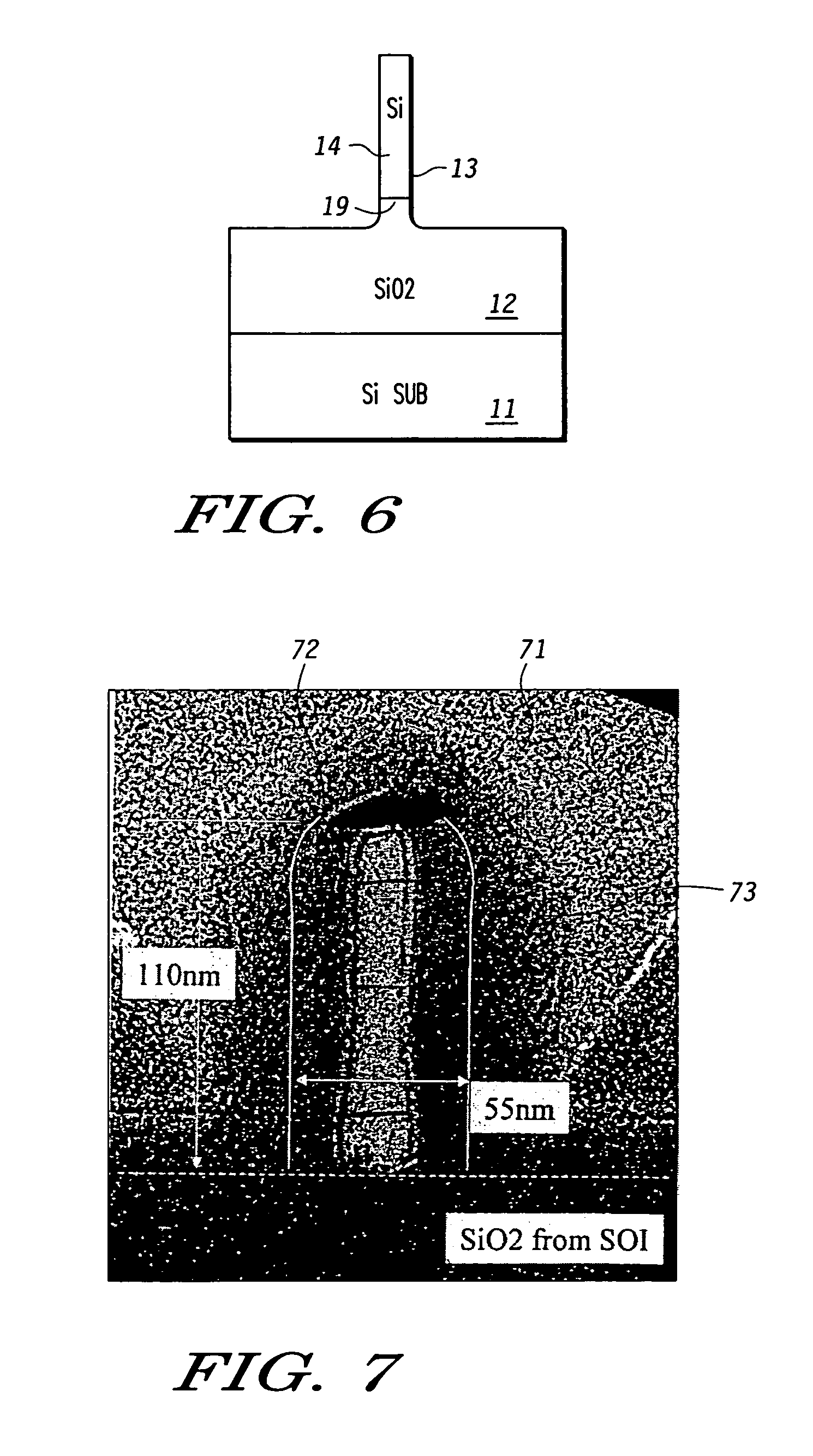
[0018]It has now been discovered that an additional process step or steps can be added during the fabrication of fin structures to avoid the above-mentioned prior art shortcomings and limitations. A diffusion layer of, for example, silicon dioxide is deposited around an oversized silicon fin. Oxygen is then allowed to diffuse through the diffusion layer, to the silicon fin, whereupon the oxygen reacts with the silicon to form silicon dioxide. Control of parameters such as the time and temperature of oxidation, and of the thickness of the diffusion layer on the sidewall of a fin structure, affects the degree of oxidation that takes place. Pro...


PUM

PropertyMeasurementUnit
temperatureaaaaaaaaaa
widthaaaaaaaaaa

Abstract

The present invention provides a method of fabricating a silicon fin useful in preparing FinFET type semiconductor structures. The method is particularly useful for creating fins with a width and smoothness appropriate for sub-50 nm type gates. The method begins with a silicon fin prepared by lithographic means from an SOI type structure such that the fin is larger in dimension, particularly width, than is desired in the final fin. If desired the silicon fin can include a nitride cap. A conformal diffusion layer, such as of silicon dioxide, is then deposited onto the fin and silicon dioxide substrate. A PECVD deposition using TEOS gas is one method to deposit the diffusion layer. The coated fin is then heated and exposed to oxygen. The oxygen diffuses through the diffusion layer and converts a portion of the silicon material to silicon dioxide. This oxidation continues until a desired amount of silicon material is converted to SiO2 such that the remaining silicon has the desired dimensions. The silicon fin is then exposed through wet etching steps that remove the silicon dioxide coating.

Description

FIELD OF THE INVENTION[0001]The present invention relates to a method of forming very thin fins for use on FinFET devices. The present invention more particularly relates to deposition of a diffusion layer on a predeposited silicon fin to act as a controlling agent in the oxidation of silicon to SiO2. The diffusion of oxygen through the diffusion layer yields a silicon fin with thin walls, desired dimensions, and good mechanical strength.BACKGROUND OF THE INVENTION[0002]Metal Oxide Semiconductor Field Effect Transistors (MOSFETs) have found a wide application as electronic devices. They find significant use, for example, in digital processing applications. MOSFETS, like other transistor devices, continue to be scaled to smaller and smaller dimensions in order to improve integrated circuit performance and cost. As the MOSFET device is further miniaturized, however, it becomes increasingly difficult to maintain high performance characteristics. It also becomes increasingly technically...

Claims


Application Information

Patent Timeline
Patent Type & Authority Patents(United States)
IPC IPC(8): H01L21/336H01L21/02H01L21/70H01L21/338H01L21/84H01L21/316H01L29/786
CPCH01L29/66818H01L29/785H01L21/31662H01L21/02216H01L21/02274H01L21/02164H01L21/02238H01L21/02255
Inventor HAN, SANG-INEISENBEISER, KURT W.LU, BING
Owner NORTH STAR INNOVATIONS
Why Eureka
Try Eureka