Configurable electronic device with mixed granularity

Active Publication Date: 2005-11-01
STMICROELECTRONICS SRL
View PDF4 Cites 11 Cited by
  • Summary
  • Abstract
  • Description
  • Claims
  • Application Information

AI Technical Summary

Benefits of technology

[0006]An object of the present invention is to provide a configurable electronic device with mixed programming granularity, in which it is possible to use a mapping methodology similar to the metho

Problems solved by technology

Furthermore, one cannot really speak of truly arithmetic resources, since the arithmetic operators share the same routing resources as those dedicated to the bit level.
Consequently, the use of such circuits FPGA for carrying out essentially arithmetic functions is not really efficient either from a surface area standpoint or fro

Method used


Image

  • Configurable electronic device with mixed granularity
  • Configurable electronic device with mixed granularity
  • Configurable electronic device with mixed granularity

Examples


Embodiment Construction

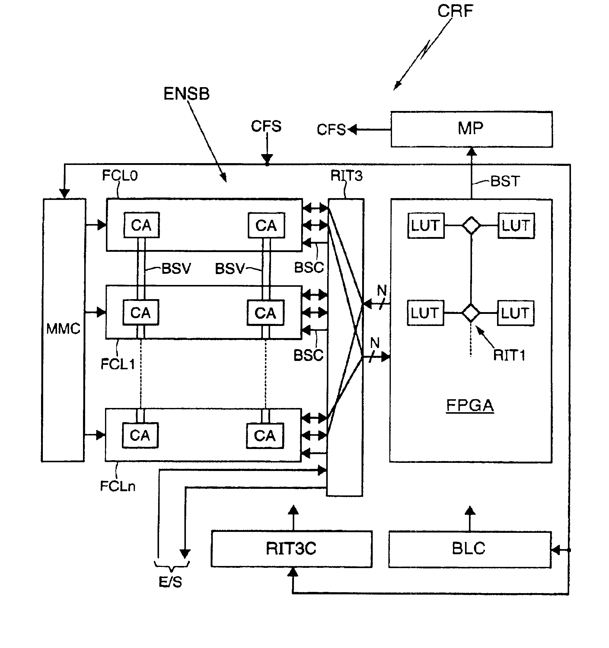
[0022]In FIG. 1, the reference CRF designates a configurable circuit according to the invention. This circuit essentially comprises in this embodiment a basic assembly ENSB comprising a programmable circuit FPGA with fine programming granularity, several groups of arithmetic cells FCL0-FCLn, and a programmable or configurable interconnection network RIT3 interconnecting the groups of cells with the circuit FPGA.

[0023]Since the programmable circuit FPGA may be a semi-custom programmable FPGA circuit, for example, the reference FPGA has been assigned to this circuit for simplifying reasons. The circuit FPGA can be one of those marketed by the company Xilinx, for example.

[0024]Although the structure and the manner of operation of such a programmable circuit FPGA are well known to the person skilled in the art, a few essential elements thereof are briefly recalled here. This circuit is formed of several programmable memories LUT (look-up tables). The memories LUT are, for example, memor...


PUM


Abstract

The configurable electronic device comprises a configurable electronic device includes at least one configurable basic assembly. The basic assembly includes a programmable circuit having a plurality of programmable elements, and a first configurable interconnection network for mutually connecting the programmable circuits. A plurality of configurable arithmetic cells are mutually connected by a second configurable interconnection network. A third configurable interconnection network links the programmable circuit and the configurable arithmetic cells. A control bus is between the programmable circuit and the configurable arithmetic cells, and also extends within the configurable arithmetic cells.

Description

FIELD OF THE INVENTION[0001]The present invention relates to configurable electronic devices, and in particular, to a configurable electronic device with mixed granularity that is dedicated to arithmetic computations involving words of common lengths.BACKGROUND OF THE INVENTION[0002]Configurable electronic circuits are defined as being formed of an elementary cell duplicated a certain number of times, and whose inputs / outputs are interconnected by a network of programmable switches. In this regard mention may be made of semi-custom programmable circuits, known as Field-Programmable Gate Array (FPGA) circuits. In FPGA circuits, the elementary cells are programmable memories or look-up tables carrying out logic operations at the bit level, that is, on a limited number of bits, for example 2 to 4 bits, and yielding a result likewise on several bits, for example 1 or 2 bits. The family of Virtex products marketed by the company Xilinx offers such FPGA circuits also comprising a few dedi...

Claims


Application Information

Patent Timeline
IPC IPC(8): G06F15/76G06F15/78H03K19/177
CPCG06F15/7867H03K19/17732H03K19/1774H03K19/17736Y02B60/1225Y02B60/1207Y02D10/00
Inventor CAMBONIE, JOEL
Owner STMICROELECTRONICS SRL
Why Eureka
Try Eureka