Digital image processing and data compression circuit

a digital image processing and data compression technology, applied in the field of image processing circuits, can solve the problems of increasing chip cost and power consumption, and achieve the effect of reducing memory cost and power consumption, and reducing the scale of buffer areas

Inactive Publication Date: 2005-11-01
MEGACHIPS
View PDF6 Cites 29 Cited by
  • Summary
  • Abstract
  • Description
  • Claims
  • Application Information

AI Technical Summary

Benefits of technology

[0031]Accordingly, an object of the present invention is to provide an image processing circuit capable of reducing the scale of buffer areas in a memory for remarkably reducing the cost for the memory as well as power consumption.

Problems solved by technology

While the recent digital still camera is miniaturized and reduced in weight, the aforementioned built-in memory 108 is formed by a DRAM (dynamic random access memory) or an SDRAM (synchronous DRAM) and the buffer areas 108a to 108c used in the built-in memory 108 are increased in scale to disadvantageously increase the cost for a chip as well as power consumption.

Method used


Image

  • Digital image processing and data compression circuit
  • Digital image processing and data compression circuit
  • Digital image processing and data compression circuit

Examples


embodiment 1

[0056]

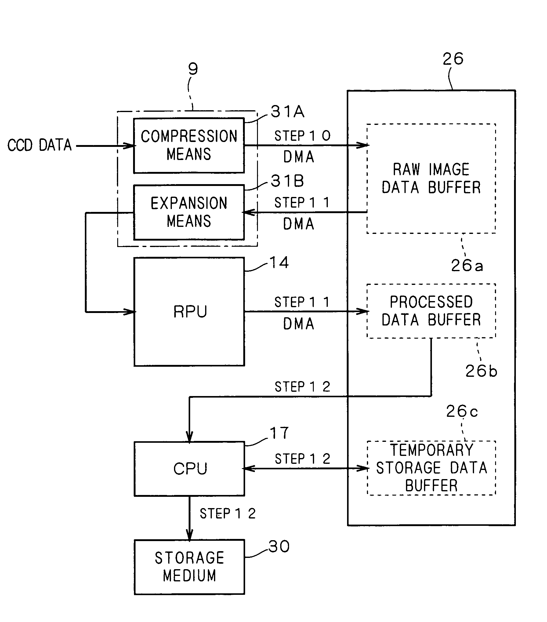
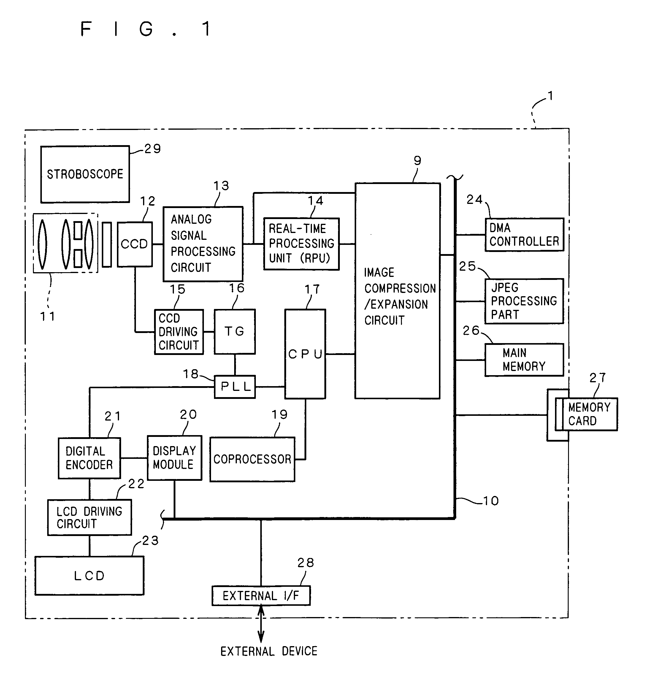
[0057]FIG. 3 is a schematic block diagram showing the flow of image signal processing by an image processing circuit according to an embodiment 1 of the present invention in the digital still camera (image pickup device) 1 having the aforementioned structure.

[0058]As shown in FIG. 3, CCD data (raw image data) picked up with the CCD 12 is A / D converted to a digital image signal in the aforementioned analog signal processing circuit 13, thereafter compressed by compression means 31A of the aforementioned image compression / expansion circuit 9 by binary arithmetic coding or entropy coding such as Huffman coding and transferred to a raw image data buffer 26a provided in the main memory 26 through the aforementioned main bus 10 to be temporarily stored therein (step 10). The CCD data may be output by either the interlacing system or the progressive system.

[0059]Then, the compressed data stored in the raw image data buffer 26a is expanded in expansion means 31B of the aforementioned ...

embodiment 4

[0080]

[0081]FIG. 7 is a schematic block diagram showing the flow of image signal processing in an image processing circuit according to an embodiment 4 of the present invention prepared by improving the aforementioned embodiment 3. The feature of this embodiment resides in that the image processing circuit comprises a selector 33 switching the destination of connection of compression means 31A to either division means 32 or a CPU 17 and the CPU 17 executing a defect inspection of a block expanded in expansion mean 31B and defect correction by software processing.

[0082]As shown in FIG. 7, A / D converted CCD data is input in the division means 32 of an image compression / expansion circuit9, and divided into a plurality of blocks having a prescribed bit length in real time (step 40). A divided image signal is input in the aforementioned compression means 31A through the selector 33, compressed in units of blocks by entropy coding or the like, and transferred to and temporarily stored in ...

embodiment 7

[0093]

[0094]FIGS. 10A and 10B show another exemplary differential compression according to an embodiment 7 of the present invention. FIG. 10A is a schematic diagram for illustrating the differential compression according to the embodiment 7, and FIG. 10B is a schematic block diagram showing an exemplary structure implementing the differential compression. As shown in FIG. 10B, A / D converted CCD data is input in difference calculation means 44, which in turn calculates the difference between the values of alternate pixels along the time base in each line forming a frame for converting the CCD data to differential data. As shown in FIG. 10A, the difference calculation means 44 calculates the differences between pixel values of the same color components between alternate pixels 401 and 403, 402 and 404, 403 and 405, . . . in pixels 401, 402, 403, . . . forming CCD data of a single line for generating differential data. Then, compression means 31A performs reversible coding such as entr...


PUM


Abstract

CCD data is compressed by compression means and stored in a raw image data buffer (step 10). Then, the compressed data is expanded by expansion means, so that pixel data thereof is sequentially output to an RPU (step 11). The RPU executes real-time image processing on the pixel data, so that the processed data is stored in a processed data buffer in units of frames. Then, a CPU reads an image from the processed data buffer at a proper timing and performs software processing such as high-efficiency coding through a temporary storage data buffer, for storing and preserving the processed data in a storage medium (step 12). Thus provided is an image processing circuit capable of reducing the scale of buffer areas in a memory for remarkably reducing the cost for the memory as well as power consumption.

Description

BACKGROUND OF THE INVENTION[0001]1. Field of the Invention[0002]The present invention relates to an image processing circuit for image-processing image data picked up with an image pickup device such as a digital still camera.[0003]2. Description of the Background Art[0004]FIG. 13 schematically illustrates the structure of a general digital still camera 100. As shown in FIG. 13, an image signal picked up with an image pickup device 105 such as a loaded CCD or CMOS sensor is A / D converted to a digital image signal and thereafter captured by an image processing part 106, to be subjected to various image processing such as pixel interpolation, color space conversion and contour correction. The image data subjected to the image processing is displayed on a finder of a liquid crystal monitor 109 or the like, stored in a memory card 110 or output to an external device such as a personal computer through an interface 111. Referring to FIG. 13, numeral 101 denotes an optical lens, numeral 1...

Claims


Application Information

Patent Timeline
Patent Type & Authority Patents(United States)
IPC IPC(8): H04N5/217H04N5/335H04N1/21H04N5/14H04N1/41H04N5/232H04N5/361H04N5/367H04N5/378H04N9/64H04N19/00H04N19/423H04N19/426H04N101/00
CPCH04N5/2176H04N5/335H04N25/63H04N25/00
Inventor SASAKI, GEN
Owner MEGACHIPS
Why Eureka
Try Eureka