Semiconductor laser device

a laser device and semiconductor technology, applied in semiconductor lasers, laser details, electrical devices, etc., can solve the problems of laser characteristics deteriorating at the time of high-output operation, etc., to achieve low drive voltage, high kink level, and large value of //

Inactive Publication Date: 2005-11-01
SONY CORP
View PDF12 Cites 20 Cited by
  • Summary
  • Abstract
  • Description
  • Claims
  • Application Information

AI Technical Summary

Benefits of technology

[0023]It is an object of the present invention to provide a semiconductor laser device of ridge waveguide type which has a low drive voltage, a large value of θ / / , and a high kink level or good light output-injected current characteristics up to a high output range.

Problems solved by technology

Unfortunately, any attempt to increase the value of Δn ends up with a narrow cutoff ridge width of high-order horizontal lateral mode.
The result is a deterioration in the laser characteristics at the time of high-output operation.
As mentioned above, any attempt to increase the value of Δn, thereby increasing the value of θ / / , ends up with a decreased cutoff ridge width, which leads to a deterioration in laser characteristics at the time of high-output operation.
However, this suffers the disadvantage that the ridge width exceeds the cutoff ridge width, resulting in a deterioration in the laser characteristics at the time of high-output operation.
As mentioned above, the related-art nitride based semiconductor laser device poses several problems.
That is, it does not permit the ridge width to be decreased appreciably in order to keep its drive voltage low.

Method used


Image

  • Semiconductor laser device
  • Semiconductor laser device
  • Semiconductor laser device

Examples


embodiment 1

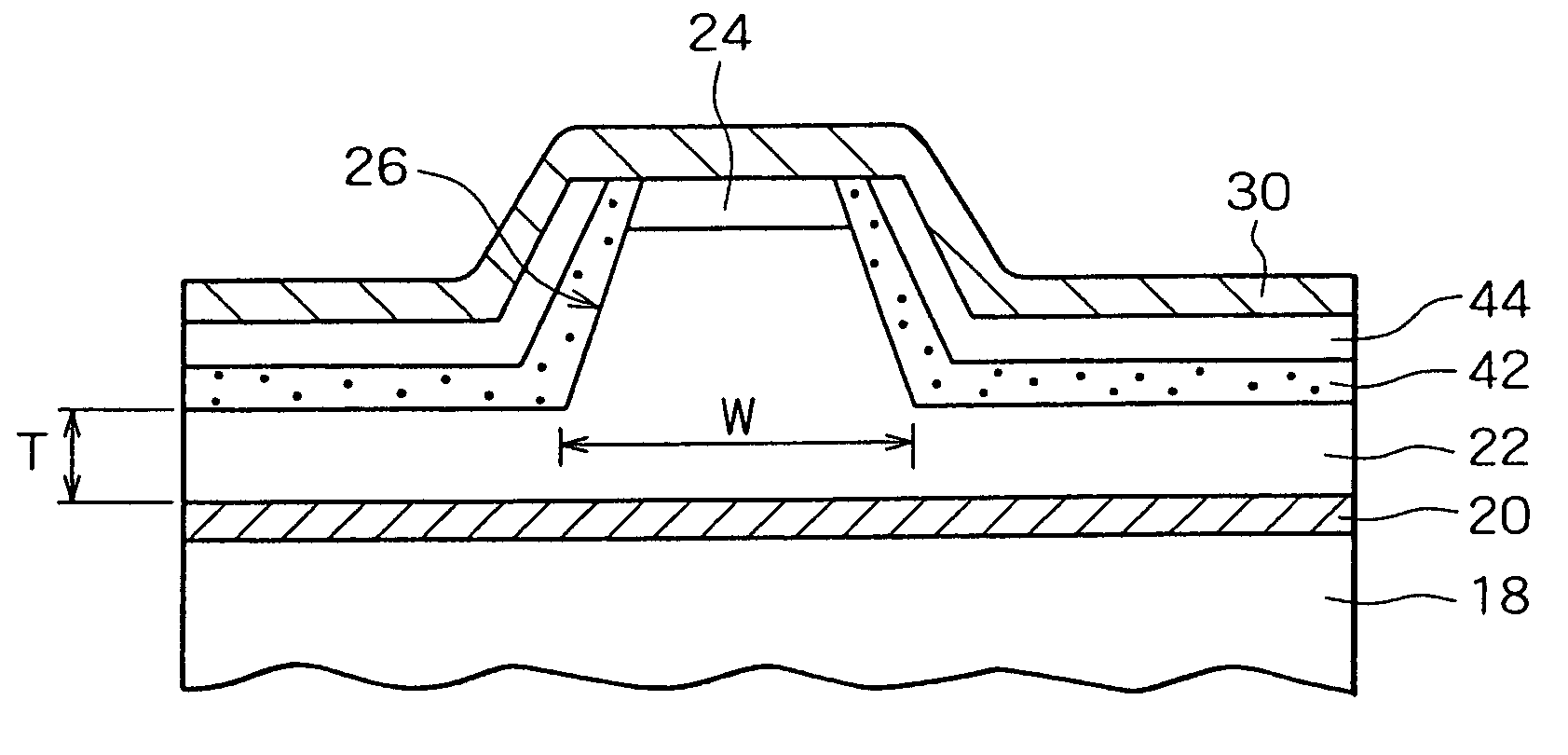
[0061]The present invention is embodied in a nitride based III-V group compound semiconductor laser device (referred to as “nitride based semiconductor laser device” hereinafter), which consists of essential parts shown in a sectional view in FIG. 1.

[0062]The nitride based semiconductor laser device consists of a substrate and a resonator structure composed of a nitride based III-V group compound semiconductor layer formed on the substrate. A ridge is formed in an upper layer of an upper cladding layer of AlGaN on the nitride based semiconductor laser device. The nitride based semiconductor laser device is similar in structure to the related-art nitride based semiconductor laser device 10 shown in FIG. 11, except for the current constricting layer on the upper cladding layer 22 extending sideward from the base of the ridge 26.

[0063]In this embodiment, the current constricting layer on the upper cladding layer 22 is a stacked film, formed on both sides of the ridge, composed of an Si...

example 1

[0074]A concrete example of Embodiment 1 is illustrated by a sample of a nitride based III-V group compound semiconductor laser device having an oscillation wavelength of around 410 nm. This sample has the same structure as the related-art semiconductor laser device 10 shown in FIG. 11 except for the current constricting layer in the ridge 26. As in the related-art semiconductor laser device 10, the width of the ridge 26 is 1.7 μm and the thickness of the p-AlGaN cladding layer 22 extending sideward from the base of the ridge 26 is 0.17 μm.

[0075]The sample in this example has a stacked film composed of an SiO2 film 42 (600 Å thick) and an amorphous Si film 44 (300 Å thick), which are sequentially formed by vapor deposition. This stacked film covers the sides of the ridge 26 and the p-AlGaN cladding layer 22 extending sideward from the base of the ridge 26. The stacked film has a window through which the p-side electrode 30 is electrically connected to the p-GaN contact layer 24.

[007...

embodiment 2

[0077]The second embodiment of the present invention is a nitride based semiconductor laser device whose essential parts are constructed as shown in a sectional view in FIG. 5.

[0078]The sample in this embodiment is similar in structure to that in Embodiment 1 except for the current constricting layer in the ridge 26. The sample in this embodiment has a stacked film composed of an SiO2 film 46 as an insulating film and a p-side electrode 30 as an absorption film, sequentially. As shown in FIG. 5, this stacked film covers the sides of the ridge 26 and the p-AlGaN cladding layer 22 extending sideward from the base of the ridge 26.

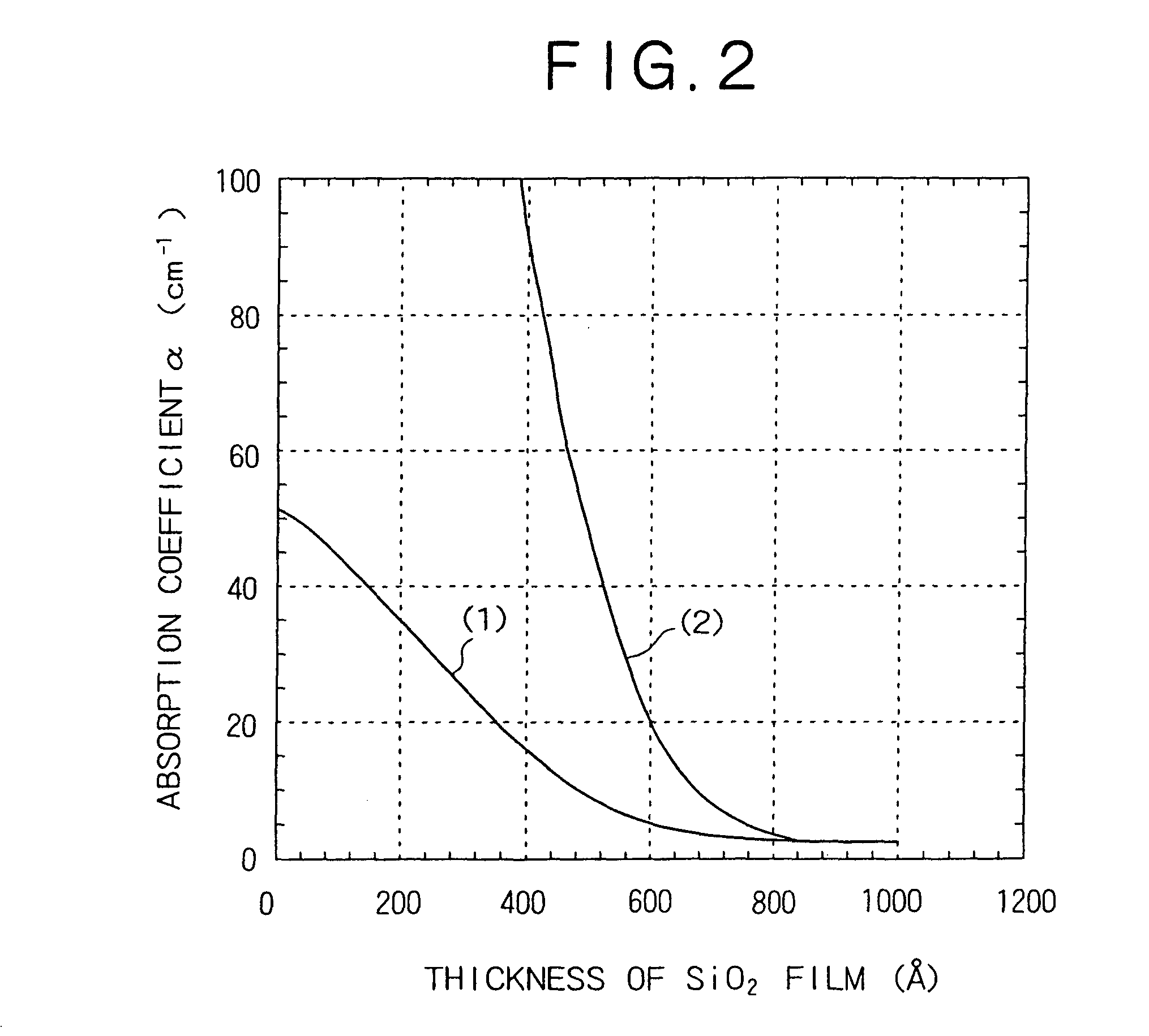
[0079]For the purpose of evaluation, several samples were prepared in which the p-side electrode 30 has a fixed thickness (40 nm) and the SiO2 film 46 has a varied thickness. They were tested for change in the absorption coefficient of fundamental horizontal lateral mode and the absorption coefficient of primary horizontal lateral mode. The results are shown i...


PUM


Abstract

Disclosed is a nitride based III-V group compound semiconductor laser device of ridge waveguide type with an oscillation wavelength of about 410 nm which has a low driving voltage, a high half-width value θ// of a FFP in a direction horizontal to a hetero interface, and a high kink level (i.e., good light output-injected current characteristics over the high-output range). This laser device is similar in structure to the related-art semiconductor laser device except for the current constricting layer formed in a ridge. It has a stacked film composed of an SiO2 film (600 Å thick) and an amorphous Si film (300 Å thick) which are formed on the SiO2 film by vapor deposition. The stacked film covers both sides of the ridge and a p-AlGaN cladding layer extending sideward from the base of the ridge. The SiO2 film and Si film have respective thicknesses which are established such that the absorption coefficient of fundamental horizontal lateral mode is larger than the absorption coefficient of primary horizontal lateral mode. This structure results in a higher kink level, while suppressing the high-order horizontal lateral mode, a larger effective refractive index difference Δn, and a larger value of θ// without the necessity for reducing the ridge width.

Description

[0001]The present application is a divisional of U.S. application Ser. No. 10 / 120,566 filed Apr. 11, 2002, now U.S. Pat. No. 6,711,197 which claims priority to JP 2001-114268, filed Apr. 12, 2001, both of which are incorporated herein by reference to the extent permitted by law.BACKGROUND OF THE INVENTION[0002]The present invention relates to a semiconductor laser device of ridge waveguide type. More particularly, the present invention relates to a semiconductor laser device of ridge waveguide type which has a desirably controlled half-width value θ / / of a far field pattern (FFP) in a direction horizontal to a hetero interface, exhibits good laser characteristics during high-output operation and merely requires a low driving voltage.[0003]Semiconductor laser devices of ridge waveguide type, including those which are based on GaAs or InP for long wavelengths and a nitride based III-V group compound for short wavelengths, find use in a various application areas because they are easy t...

Claims


Application Information

Patent Timeline
Patent Type & Authority Patents(United States)
IPC IPC(8): H01S5/00H01S5/22H01S5/323
CPCH01S5/22H01S5/0655H01S5/2218H01S5/2219H01S5/32341
Inventor TOJO, TSUYOSHIUCHIDA, SHIROKIJIMA, SATORU
Owner SONY CORP
Why Eureka
Try Eureka