

Adaptive antenna optimization network
- Summary
- Abstract
- Description
- Claims
- Application Information
AI Technical Summary
Benefits of technology
Problems solved by technology
Method used
Image

Examples
second embodiment
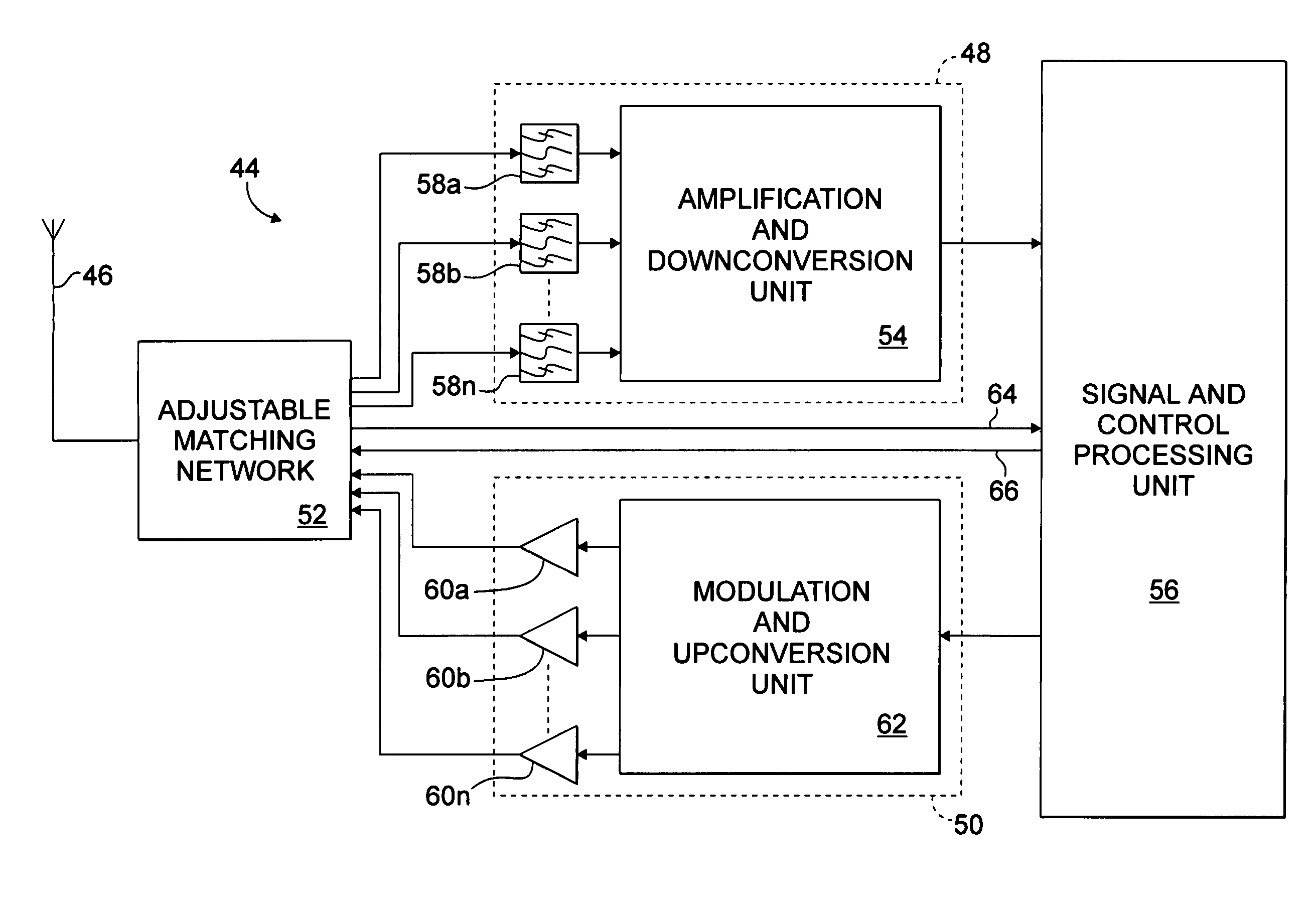
[0053]FIG. 6 illustrates the adjustable matching network, shown generally at 52′. The adjustable matching network 52′ includes a variable matching network 84 connected between the antenna 46 and the T / R switch 68. The bank of switches 72 is connected to the T / R switch 68 in the same manner as previously described with respect to FIG. 5. However, the receive 78a–n and the transmit 80a–n matching networks of FIG. 5 are removed and each of the switches in the upper bank of switches 74 is connected directly to its respective band filter 58a–n and, similarly, each of the switches in the lower bank of switches 76 is connected to its respective power amplifier 60a–n. Control signals 86 from the signal and control processing unit 56 operate the I / R switch 68 at the TDMA frame rate, but operate the bank of switches 72 and the variable matching network 84 only when changing frequency bands. Although it is possible to alter the variable matching network 84 between transmit and receive states, ...
third embodiment
[0054]FIG. 7 illustrates the adjustable matching network, shown generally at 52″, that permits cross-band operation. The adjustable matching network 52″ includes separate variable receive 88 and transmit 90 matching networks for matching the receiver separately from the transmitter. The T / R switch 68 is connected to the antenna 46, with the variable receive matching network 88 connected to the receiver contact of the T / R switch 68, and the variable transmit matching network 90 connected to the transmit contact of the T / R switch 68. The variable receive matching network 88 is connected to the upper bank of switches 74 to match the antenna 46 to the appropriate receive band filter 58a–n. Similarly, the variable transmit matching network 90 is connected to the lower bank of switches 76 for matching the antenna 46 to the appropriate power amplifier 60a–n. Thus, the selection of the transmit band and the receive band are independent, permitting cross-band operation without the need to al...
PUM
 Abstract
Description
Claims
Application Information