System for intellectual property reuse in integrated circuit design

a technology of integrated circuit design and intellectual property, applied in the field of reusable circuit design components, can solve the problems of inability to meet the needs of users, physical circuits that do not behave like ideals, and design that works as a model may not work when produced as a physical devi

Inactive Publication Date: 2005-11-01
SIEMENS PROD LIFECYCLE MANAGEMENT SOFTWARE INC
View PDF4 Cites 55 Cited by
  • Summary
  • Abstract
  • Description
  • Claims
  • Application Information

AI Technical Summary

Benefits of technology

[0019]Standard component types are defined. Each component in the system is of a standardized type. The attributes, deliverables, and qualification standards for each type of component are controlled in the system. Thus, a designer wishing to reuse a component can be assured that the component is uniformly characterized with regard to its attributes and its qualifications. The object-oriented aspect of defining component types and then instantiating components provides an scalable system in which it is easy to create instances versions and associations of objects. While the system provides a standard framework for designers, it is flexible in that new component types, standards, attributes, and deliverables can be readily defined and added to the system by the system administrators.
[0020]By using the abstract concept of a standardized “deliverable” and characterizing each deliverable using metadata in a database separate from the design file, applicants are able to provide a system that manages a large number of different types of design files in an efficient manner that allows other designers to understand and reuse the files.
[0021]The use of the deliverables concept allows the system to provide a hierarchical configuration management by maintaining a hierarchy of components and provides version control that provides for versions for each deliverable and subcomponent of a component as well as a single version for the component itself. The combination of the component model and the data structure of design files and metadata files produces a knowledge management system that is suitable for managing an extensive knowledge base.

Problems solved by technology

Integrated circuit design and manufacturing are incredibly complex operations.
The physical circuit does not behave like ideal, theoretical components so a design that works as a model may not work when produced as a physical device.
One consequence of decreased feature sizes is that there is an ever-increasing amount of space available on the silicon die that can be used for circuitry.
While the productivity of circuit designed is estimated to be increasing at about twenty percent a year, this is insufficient to take advantage of the available space on the chips in time to meet the market demand.
Designers are not able to keep up with the increased capacity of the chips.
For example, many semiconductor houses have the silicon process complexity to put more than 20 million logic gates on a chip.
It is widely recognized that a productivity gap exists between the capabilities of today's electronic design automation (EDA) tools and the number of gates available on a single die in the current silicon processes.
Even with this understanding, limited design reuse has been occurring so far.
One barrier to design reuse is the technical challenges involved in sharing IP between design groups.
Although some individual design groups have created standardized directory formats for different file types, there has been no standards across the industry or even across most companies.
When a design is provided to another designer, there has been no standardization regarding how the files are named or organized, so it can be difficult to determine where all the necessary files are located.
To complicate matters, the productivity issue driving design reuse is not only a design creation gap.
It is also a design verification gap.
It is difficult to keep track of all the different versions of the multiple files to keep track of what files are currently used in a design.
For groups of engineers sharing design data, there are also issues like incompatible tools and lack of communication.
If one designer tries to use a design created by another designer, the difference in tools or versions of tools may introduce errors in reprocessing the files.
If the original designers are not available to explain the design files, it can be impractical to re-engineer a legacy block from one technology to the next, and may be prohibitive.
Beyond the technical barriers to design reuse, there are also very real economic barriers to the initial adoption of design reuse.
For example, a design manager may find it difficult to justify designing a new block for reuse while trying to maintain the SoC design schedule.
The extra work required to make the design reusable uses up limited resources and jeopardizes the existing project.
At the same time, the existing design group may never reuse this block, making the choice of designing for reuse one of known risk for uncertain reward.
This barrier can only be overcome when the time saved reusing existing blocks in an SoC design more than makes up for the effort required to design new blocks in a usable manner.
Other barriers to design reuse are cultural in nature.
Even within a given organization, designers attempting to reuse will find incompatible deliverable formats, mismatched block interfaces, incomplete documentation and inconsistent tool flows.
Moreover, in many cases, there is no clear definition of what it means for a block to be reusable.
Additionally, with growing chip complexity, functional verification is also a formidable barrier to design reuse.

Method used


Image

  • System for intellectual property reuse in integrated circuit design
  • System for intellectual property reuse in integrated circuit design
  • System for intellectual property reuse in integrated circuit design

Examples


Embodiment Construction

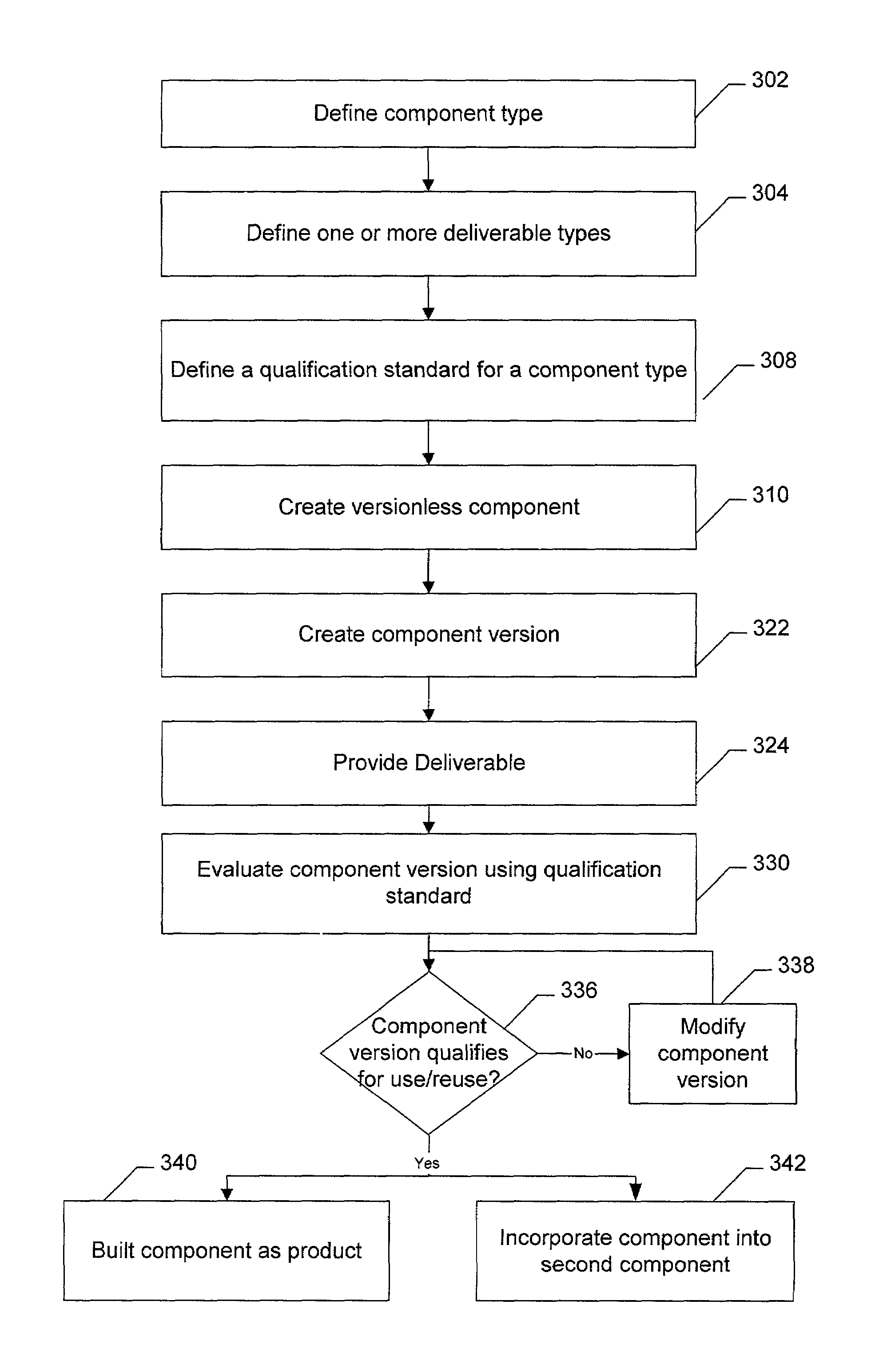
[0027]A system for creating and managing reusable IP designs and using the IP in other IP and in system-on-chips designs is described. In the following description, for purposes of explanation, numerous specific details are set forth in order to provide a thorough understanding of the present invention. It will be evident, however, to one skilled in the art that the present invention may be practiced without these specific details.

[0028]To facilitate understanding of the invention, applicants first define terminology and describe certain aspects of the invention in more detail.

Definitions, Concepts, and Structure

Intellectual Property (IP)

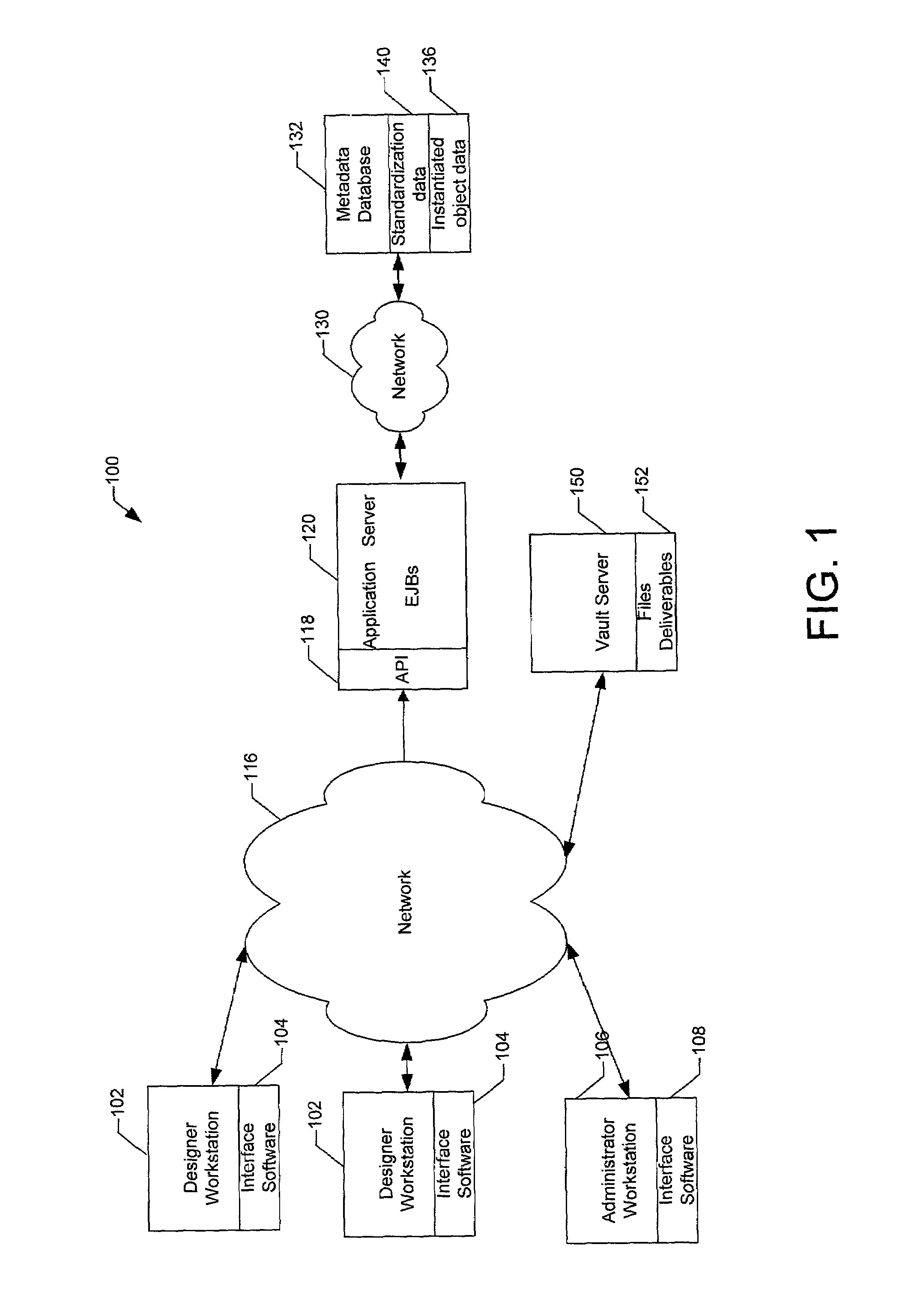
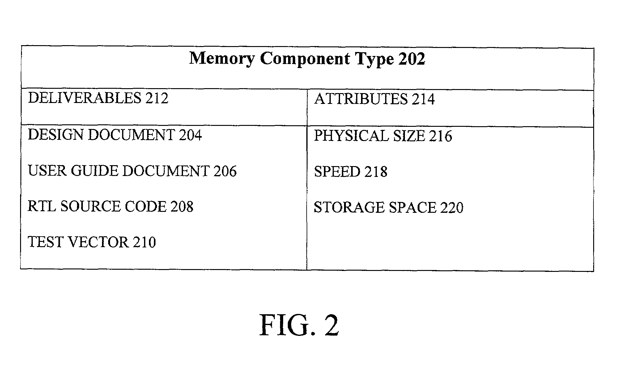
[0029]The commonly used term IP represents a particular reusable design block such as a CPU, a timer, or a complete SoC. The invention can support more than just IP components; it can be configured to store virtually any type of component.

Component

[0030]The term “component” is used to mean a reusable design block typically supported by both meta dat...


PUM


Abstract

The invention provides a knowledge management system particularly suited for use in the integrated circuit design environment. The system allows administrators to define standardized component types. Instantiated components versions comprise “deliverables” and “attributes.” Deliverables comprise a file or directory of files or groups of files or directories that perform a common function and are characterized by the system in a standardized manner. Attributes comprise metadata describe the component version. By the abstraction of design files into deliverables, the systems can work with design files originating from any source and having different structures and still make those design files available by other designers in a uniform manner for efficient reuse of pre-qualified components. Tasks in the design flow can be tracked in the system. The system may also include a communications application, an issue tracking application, and an audit trail application.

Description

RELATED APPLICATIONS[0001]This application claims priority from U.S. Provisional Patent Application No. 60 / 213,207, entitled “System for Reuse in System-On-Chip Designs,” filed Jun. 21, 2000, which is hereby incorporated by reference.FIELD OF THE INVENTION[0002]The invention relates to reusable circuit design components. More specifically, the invention relates to a system and method for creating and managing design components that can be readily inserted into circuit designs, including system-on-chip (SoC) designs.BACKGROUND OF THE INVENTION[0003]Integrated circuit design and manufacturing are incredibly complex operations. A circuit design, which begins as a functional description of circuit logic, must be converted into circuit components, such as transistors, resistors, capacitors, and connecting wires, formed from areas of conductors, semiconductors, and insulators on a semiconductor silicon die. Each of the steps in converting from logic to physical circuit must be verified to...

Claims


Application Information

Patent Timeline
Patent Type & Authority Patents(United States)
IPC IPC(8): G06F17/50
CPCG06F17/5045G06F2217/04G06F2217/66G06F30/30G06F2111/02G06F2115/08
Inventor GARNER, ROBERT E.GARDNER, DAVID N.JUSSEL, JEFFREYELMAN, ANNALING, DAVIDBENAVIDES, ALVARO EDUARDOMCADAMS, MARK A.
Owner SIEMENS PROD LIFECYCLE MANAGEMENT SOFTWARE INC
Why Eureka
Try Eureka