Method for manufacturing semiconductor capacitor having double dielectric layer therein

a technology of dielectric layer and semiconductor capacitor, which is applied in the direction of capacitors, semiconductor devices, electrical equipment, etc., can solve the problems of difficult to reduce the equivalent oxide thickness (tox) below, the surface of the bottom electrode, and the step coverage is inevitable deteriorated, so as to enhance the charge capacitance and the breakdown strength of the semiconductor capacitor

Active Publication Date: 2005-11-08
SK HYNIX INC
View PDF7 Cites 14 Cited by
  • Summary
  • Abstract
  • Description
  • Claims
  • Application Information

AI Technical Summary

Benefits of technology

[0016]It is, therefore, an object of the present invention to provide a method for manufacturing a semiconductor capacitor having a double dielectric l

Problems solved by technology

However, since the capacitor has a high vertical electrode structure, step coverage is inevitably deteriorated.
Thus, it is difficult to reduce an equivalent oxide thickness (Tox) below 40 Å because of its low dielectric constant.
In addition, since the method described above has limitation in applications for 256 megabytes or greater future generation DRAMs to ensure the desired capacitance of the capacitor for small cell area, a new DRAM capacitor having a high k dielectric material therein has been proposed such as tantalum oxide (Ta2O5, ∈=25), hafnium oxide (HfO2, ∈=20˜25) or the like.
First, in utilizing Ta2O5 as the dielectric layer 118 in the DRAM capacitor, there is a problem that the surface of the bottom electrode 116 is unavoidably oxidized during a post annealing process after depositing the dielectric layer 118 on the bottom electrode 116. Thus, the equivalent oxide thickness (Tox) becomes beyond about 30 Å. Additionally, there is also a drawback that leakage cur

Method used


Image

  • Method for manufacturing semiconductor capacitor having double dielectric layer therein
  • Method for manufacturing semiconductor capacitor having double dielectric layer therein
  • Method for manufacturing semiconductor capacitor having double dielectric layer therein

Examples


Embodiment Construction

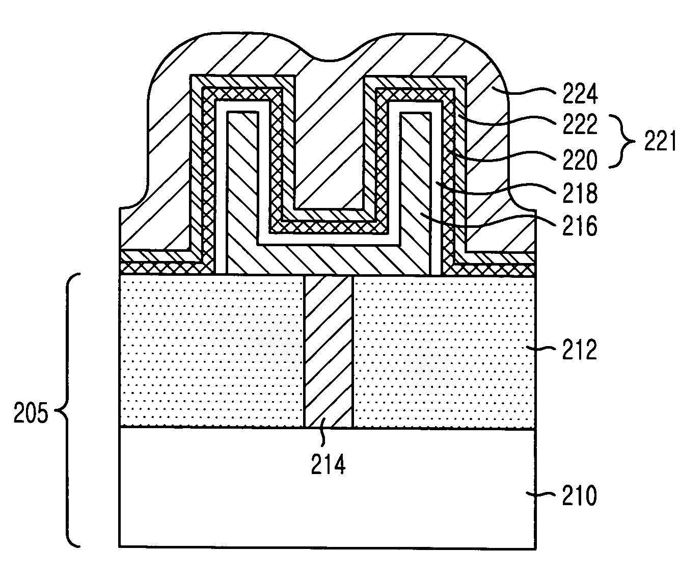
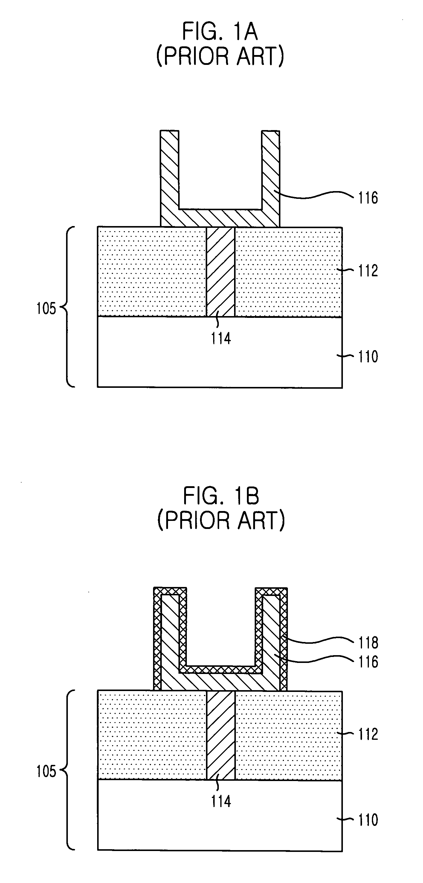
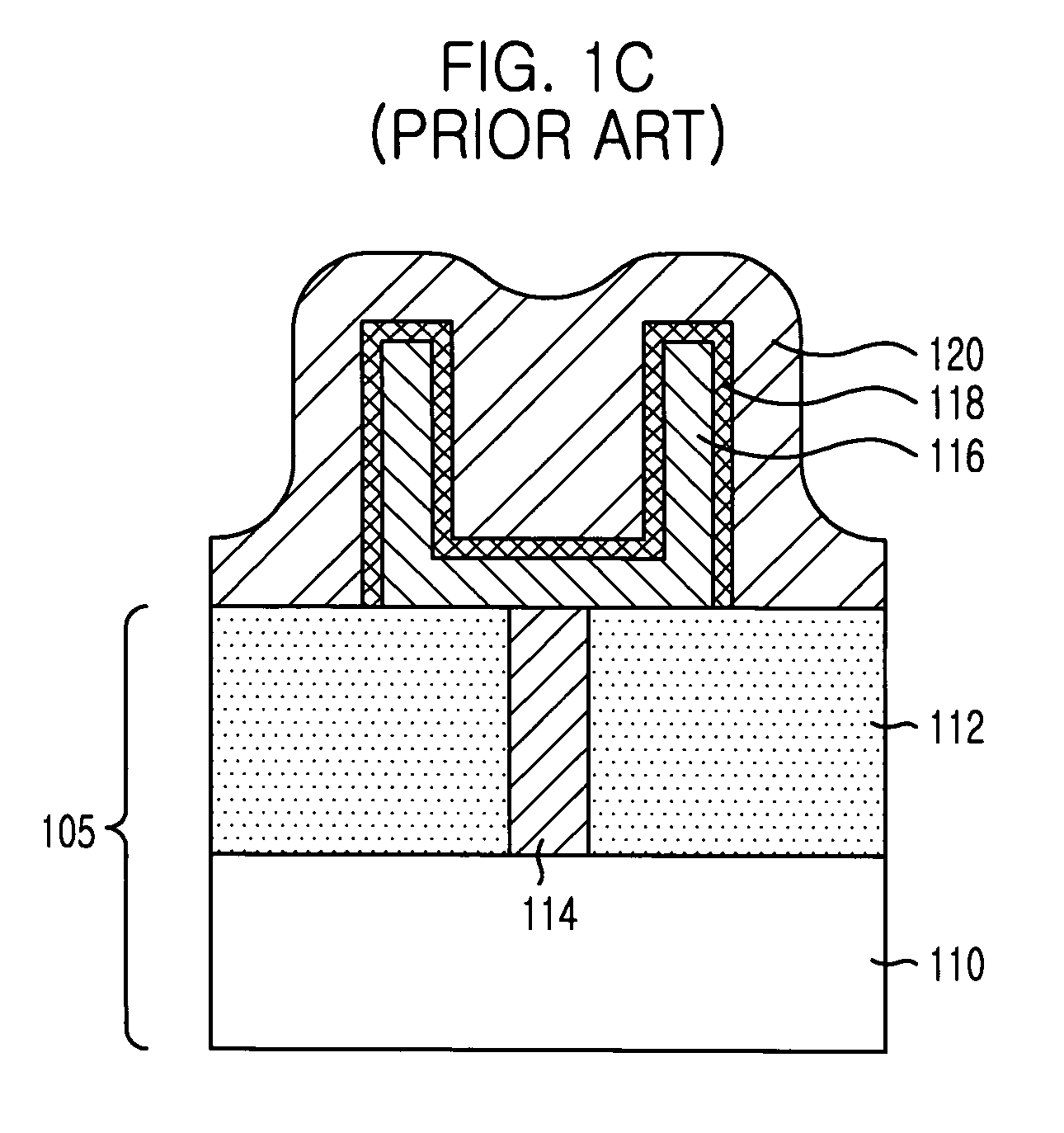
[0022]There are provided in FIGS. 2A to 2D cross sectional views setting forth a method for manufacturing a semiconductor capacitor in accordance with a preferred embodiment of the present invention. It should be noted that like parts appearing in FIGS. 2A to 2D are represented by like reference numerals.

[0023]Referring to FIG. 2A, an inventive method for manufacturing a semiconductor capacitor begins with preparation of an active matrix 205 including a semiconductor substrate 210, an ILD 212 formed on a top face of the semiconductor substrate 210 and a storage node 214 obtained after patterning the ILD 212 into a predetermined configuration. Herein, the storage node 214 employs a doped polysilicon, wherein the storage node 214 is electrically connected to a source / drain region embedded in the semiconductor substrate 210, which is not shown for the sake of convenience.

[0024]Thereafter, a bottom electrode 216 is formed on a top face of the storage node 214 and portions of the ILD 212...


PUM


Abstract

The method for manufacturing a DRAM capacitor is employed to enhance charge capacitance and electrical endurance of the DRAM capacitor by structuring a double dielectric layer of aluminum oxide (Al2O3) and hafnium oxide (HfO2). The method includes steps of: preparing an active matrix including a semiconductor substrate, an ILD formed on the semiconductor substrate and a storage node obtained after patterning the ILD into a predetermined configuration; forming a bottom electrode on top faces of the storage node and portions of the ILD; forming a diffusion barrier on an exposed surface of the bottom electrode; forming a double dielectric layer including an aluminum oxide layer and a hafnium oxide layer, wherein the aluminum oxide layer and the hafnium oxide layer are formed on the diffusion barrier in succession; carrying out an annealing process for recovering dielectric properties of the aluminum oxide layer and the hafnium oxide layer; and forming a top electrode on the hafnium oxide layer.

Description

FIELD OF THE INVENTION[0001]The present invention relates to a method for manufacturing a semiconductor device; and, more particularly, to a method for manufacturing a dynamic random access memory (DRAM) capacitor having a double dielectric layer of aluminum oxide (Al2O3) and hafnium oxide (HfO2) therein.DESCRIPTION OF THE PRIOR ART[0002]Recently, as a semiconductor device is highly integrated, research and development on the semiconductor device have been directed toward both reducing a cell area and lowering a device-operating voltage. Despite reduction of the cell area, a capacitance for operating a memory device is still demanded to be kept on the order of at least 25 fF per cell, which can prevent the memory device from generation of soft errors and decrease of a refresh time.[0003]To meet the demand, therefore, there are several methods, such as a trench type or a stack type capacitor, which are arranged three-dimensionally in the memory device for reducing the cell area avail...

Claims


Application Information

Patent Timeline
IPC IPC(8): H01L21/02H01L21/70H01L21/20H01L21/8242H01L27/108
CPCH01L28/65H01L28/75H01L27/10817H10B12/318H10B99/00
Inventor LEE, KEE-JEUNG
Owner SK HYNIX INC
Why Eureka
Try Eureka