Scanning electron microscope and sample observing method using it
a scanning electron microscope and scanning electron technology, applied in the direction of material analysis using wave/particle radiation, instruments, nuclear engineering, etc., can solve the problem of not being able to achieve stereoscopic shape, and achieve the effect of easy measuremen
- Summary
- Abstract
- Description
- Claims
- Application Information
AI Technical Summary
Benefits of technology
Problems solved by technology
Method used
Image
Examples
Embodiment Construction
[0044]The embodiment of the invention will be described with reference to the accompanying drawings.
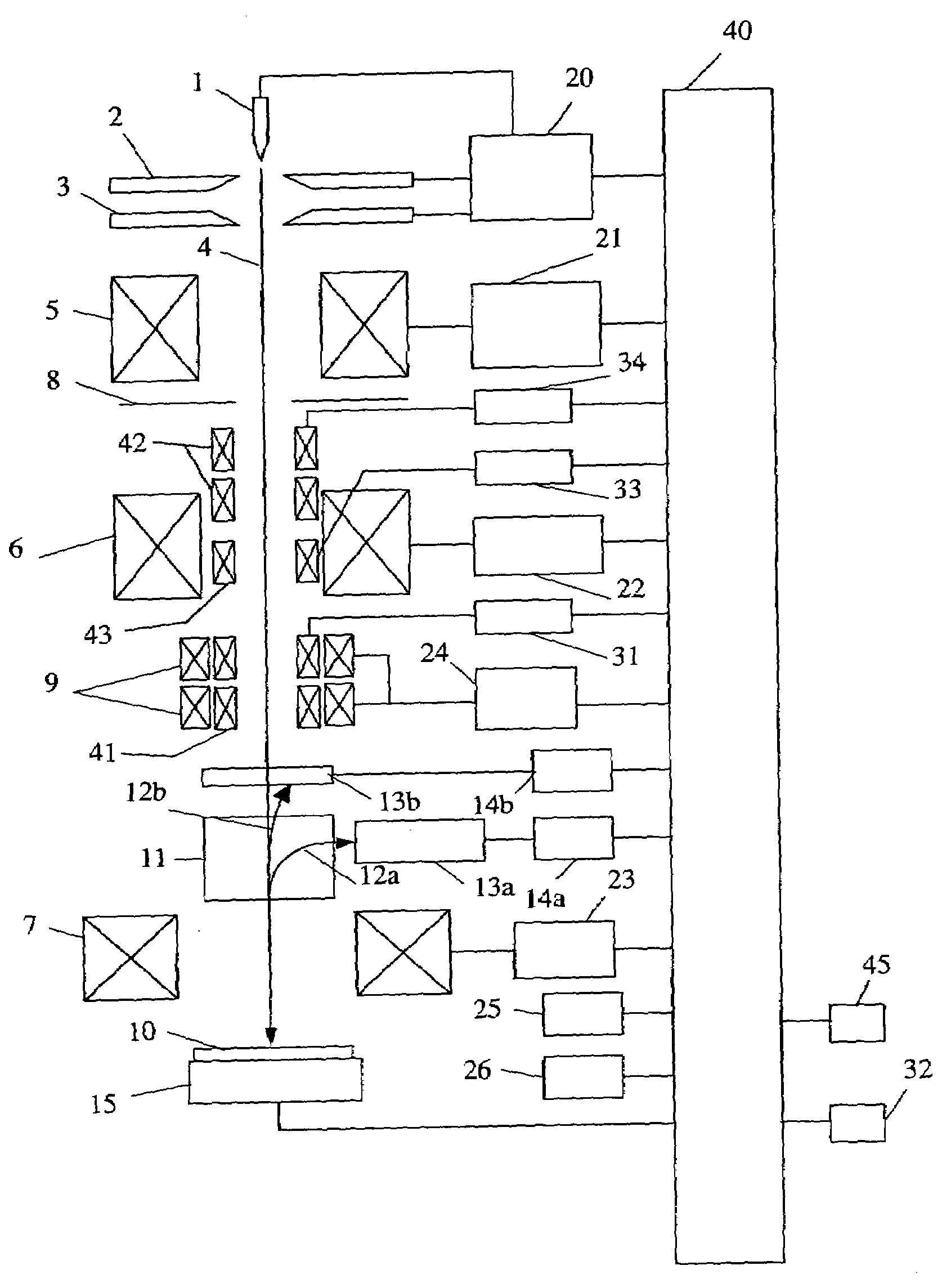
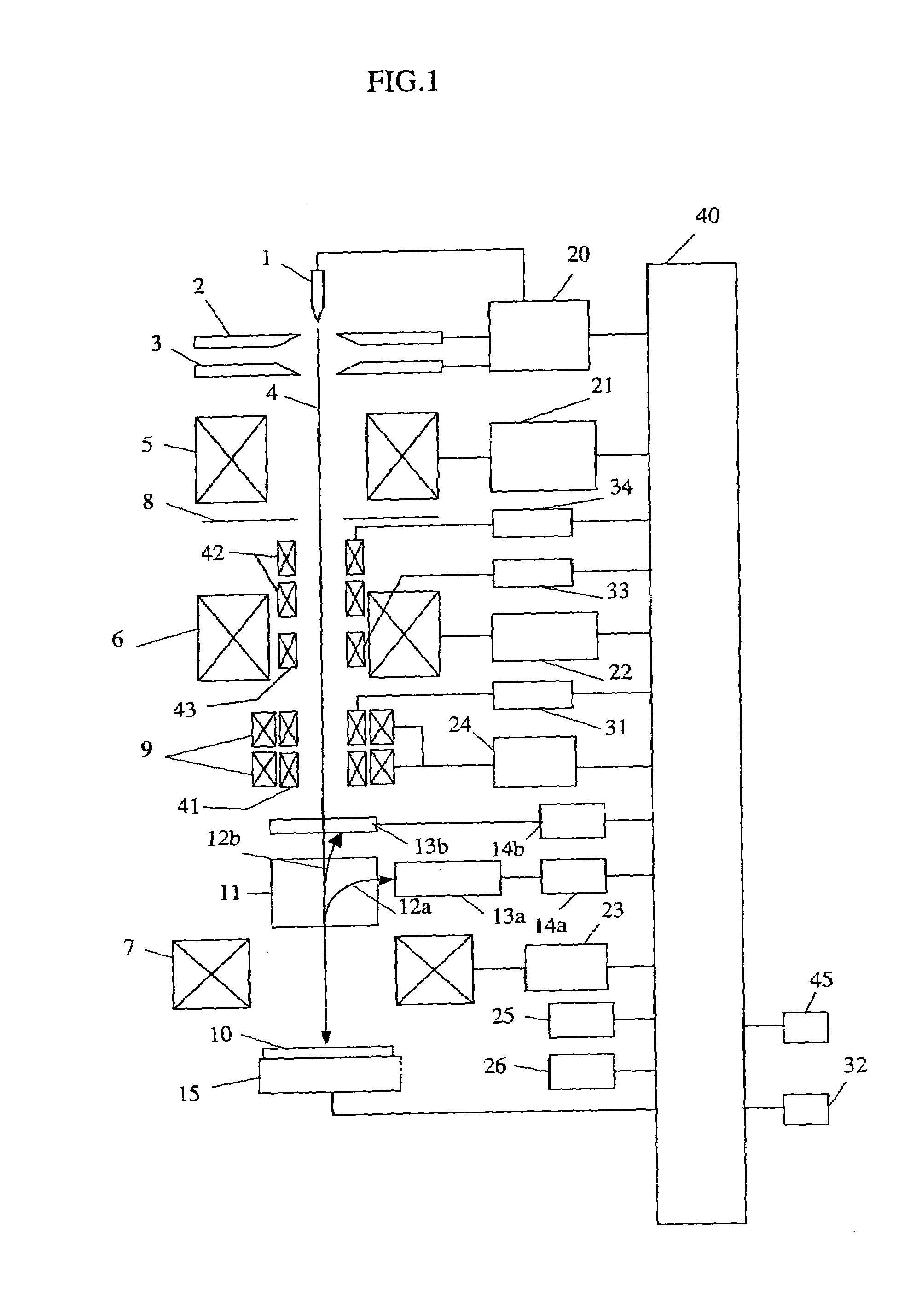
[0045]FIG. 1 illustrates a schematic configuration diagram as an example of the scanning electron microscope (SEM) according to the invention. Across a cathode 1 and a first anode 2 is applied a voltage from a power supply for high voltage control 20 controlled by a microprocessor (CPU) 40, whereby a primary electron beam 4 is induced from the cathode 1 in a predetermined emission current. Across the cathode 1 and a second anode 3 is applied an accelerating voltage from the power supply for high voltage control 20 controlled by the CPU 40, so that the primary electron beam 4 emitted from the cathode 1 is accelerated to advance to the following lens system. The primary electron beam 4 is converged by a convergent lens 5 (beam converging means) controlled by a power supply for lens control 21, and unnecessary parts of the primary electron beam are eliminated by a diaphragm 8. Thereafter...
PUM
 Abstract
Description
Claims
Application Information


