Charge pump phase locked loop with improved power supply rejection

a phase lock loop and pump technology, applied in the field of electronic circuits, can solve the problems of large area requirements, common mode problems of filters, and not often used filters in integrated applications

Active Publication Date: 2005-11-08
TEXAS INSTR INC
View PDF11 Cites 60 Cited by
  • Summary
  • Abstract
  • Description
  • Claims
  • Application Information

AI Technical Summary

Benefits of technology

[0019]Accordingly, the isolation of the circuit from the voltage signal protects the circuit from variations on the voltage source, providing and improved power supply rejection ratio of the filter.
[0021]Accordingly, the frequency output of the phase locked loop circuit is less affected by variations on the power supply.

Problems solved by technology

This type of filter is not often used in integrated applications, mainly because it requires a dual voltage supply and needs two tightly matched filters.
Also, since both inverting and non-inverting inputs are driven by the PFD 12, this filter exhibits common mode problems.
This design also is not particularly useful for integrated designs, since it requires two op-amps, which results in larger area requirements and higher noise and power consumption.
Once again, matching the filters is difficult to achieve optimum performance.
However, these devices may be difficult to integrate onto silicon die, which is highly desirable in many applications.
In addition, mismatches between sink and source devices increase the spurious level that must be filtered out with a lower bandwidth filter (again requiring a larger capacitor) and a consequently longer settling time.
Another critical issue for the traditional charge pump is the need of a complex and low noise biasing circuit and the requirements in terms of supply headroom.

Method used


Image

  • Charge pump phase locked loop with improved power supply rejection
  • Charge pump phase locked loop with improved power supply rejection
  • Charge pump phase locked loop with improved power supply rejection

Examples


Embodiment Construction

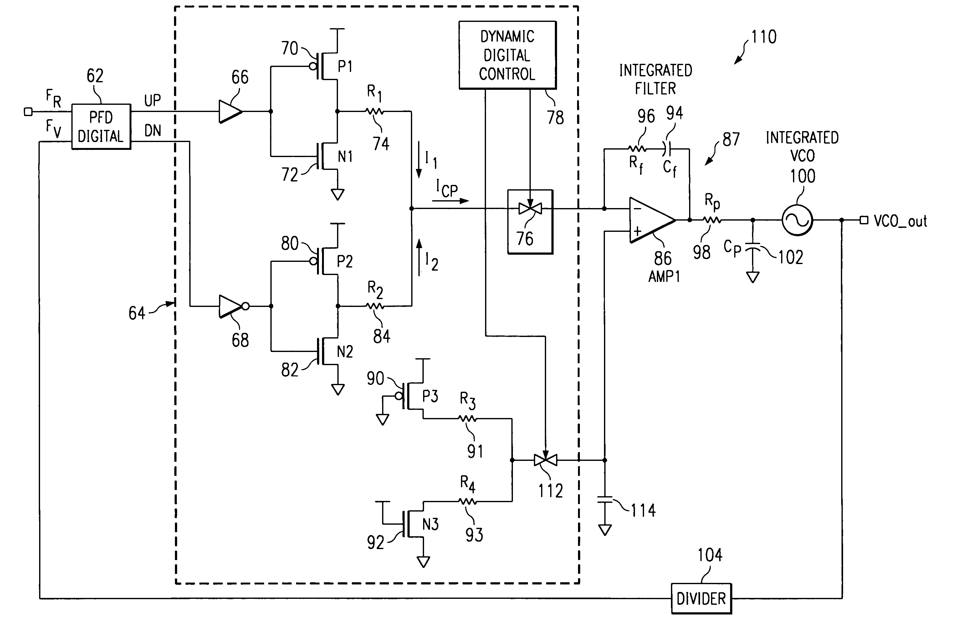
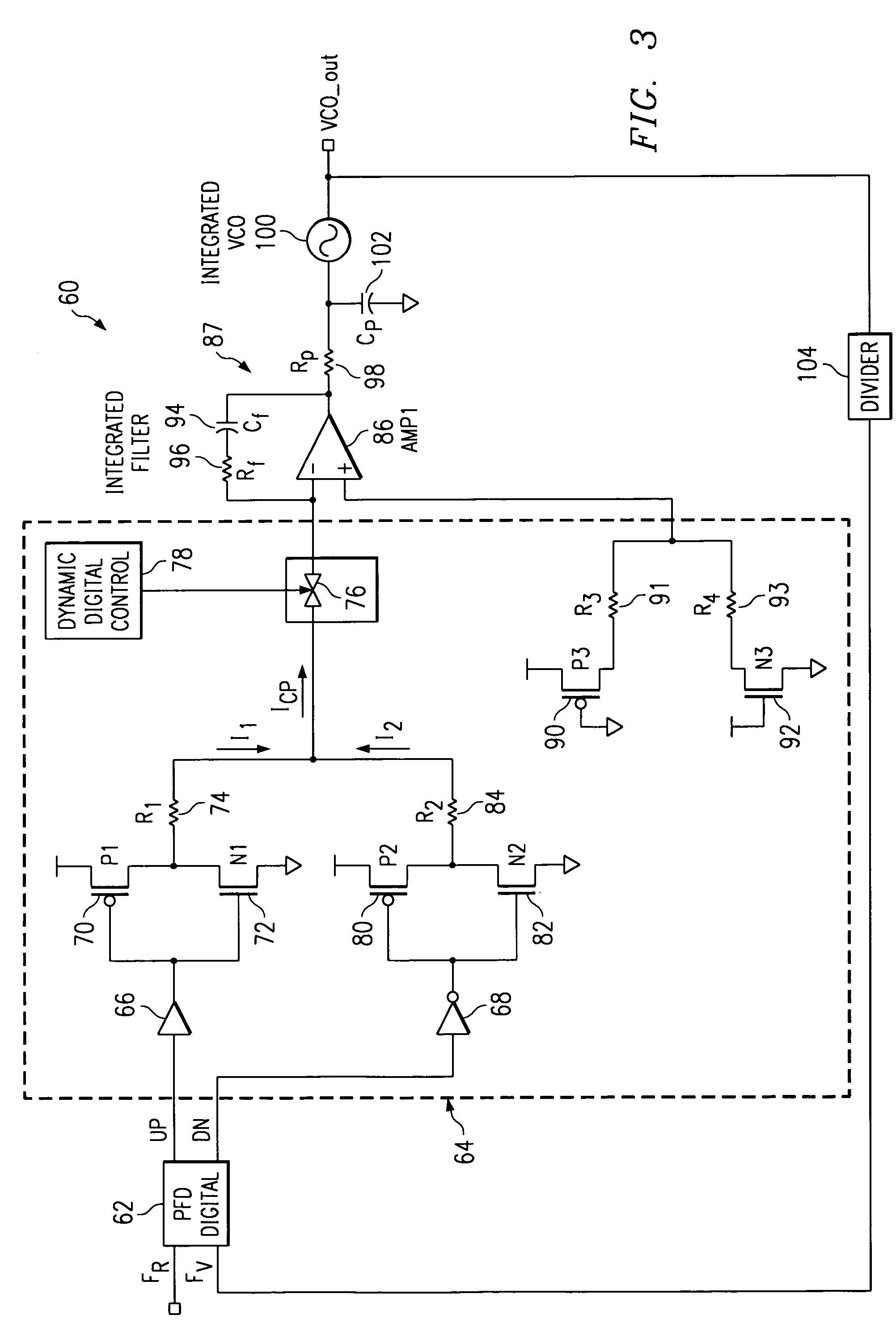
[0033]The present invention is best understood in relation to FIGS. 3–7a–b of the drawings, like numerals being used for like elements of the various drawings.

[0034]FIG. 3 illustrates a schematic diagram of a PLL 60 that can be fully integrated on a semiconductor die, with low noise characteristics, low spur levels and high linearity. A reference signal FR is input to PFD 62. PFD 62 outputs UP and DN pulses to a digital charge pump 64. The UP node of PFD 62 is coupled to a non-inverting buffer 66 and the DN node of PFD 62 is coupled to an inverting buffer 68. The output of the non-inverting buffer 66 is coupled to both gates of p-channel transistor 70 and n-channel transistor 72 that produce a logical inversion of the signal at the gates of the transistors. A first source / drain of p-channel transistor 70 is coupled to VDD and a second source / drain of p-channel transistor 70 is coupled to a first source drain of n-channel transistor 72. The second source / drain of n-channel transistor...


PUM


Abstract

A phase lock loop circuit (60) has a phase frequency detector (62), a charge pump (64), an active filter (87) and a voltage-controlled oscillator (100). The phase detector generates signals responsive to reference signal FR and VCO output signal FV. A charge pump generates a voltage at the input of a first transmission gate (76) according to the values of the phase detector signals. A predetermined voltage is generated at the input of a second transmission gate (112). When the transmission gates (76, 110) are closed (low impedance) the charge pump may sink or source current to the inverting input of the operational amplifier (86) of the active filter 86 and the predetermined voltage is applied to the non-inverting input. When the transmission gates are open (high impedance state) the inverting input is electrically isolated from the node and the non-inverting output is isolated from the power supply.

Description

CROSS-REFERENCE TO RELATED APPLICATIONS[0001]This application claims priority under 35 USC § (e)(1) of European Application Number 03292140.5 filed Aug. 29, 2003.[0002]Not ApplicableSTATEMENT OF FEDERALLY SPONSORED RESEARCH OR DEVELOPMENT[0003]Not ApplicableBACKGROUND OF THE INVENTION[0004]1. Technical Field[0005]This invention relates in general to electronic circuits and, more particularly, to phase locked loop circuits.[0006]2. Description of the Related Art[0007]A phase locked loop (PLL) synchronizes an output signal to a reference signal. Phase locked loops are used in a variety of electronic circuits for frequency synthesizing, frequency and phase modulation and demodulation, clock recovery and clock synchronization, among other uses.[0008]FIG. 1a illustrates a basic diagram of a PLL. A phase frequency detector (PFD) 12 receives two signals, FR, a reference signal, and FV, a divided-down version of the output signal. The PFD generates UP and DN (down) signals, indicating wheth...

Claims


Application Information

Patent Timeline
Patent Type & Authority Patents(United States)
IPC IPC(8): H03L7/08H03L7/06H03L7/089H03L7/00H03L7/18
CPCH03L7/0895H03L7/18
Inventor PUCCIO, GIANNIBISANTI, BIAGIOCIPRIANI, STEFANO
Owner TEXAS INSTR INC
Why Eureka
Try Eureka