

Electrode substrate and production method thereof
a technology of electrode substrate and production method, which is applied in the direction of conductive layers on insulating supports, identification means, instruments, etc., can solve the problems of insufficient electrical stability, electrode state, and inability to consider electrode state, so as to achieve the effect of reducing the existence rate of surface defects on the surface of electrodes
- Summary
- Abstract
- Description
- Claims
- Application Information
AI Technical Summary
Benefits of technology
Problems solved by technology
Method used
Image

Examples
first embodiment
[First Embodiment]
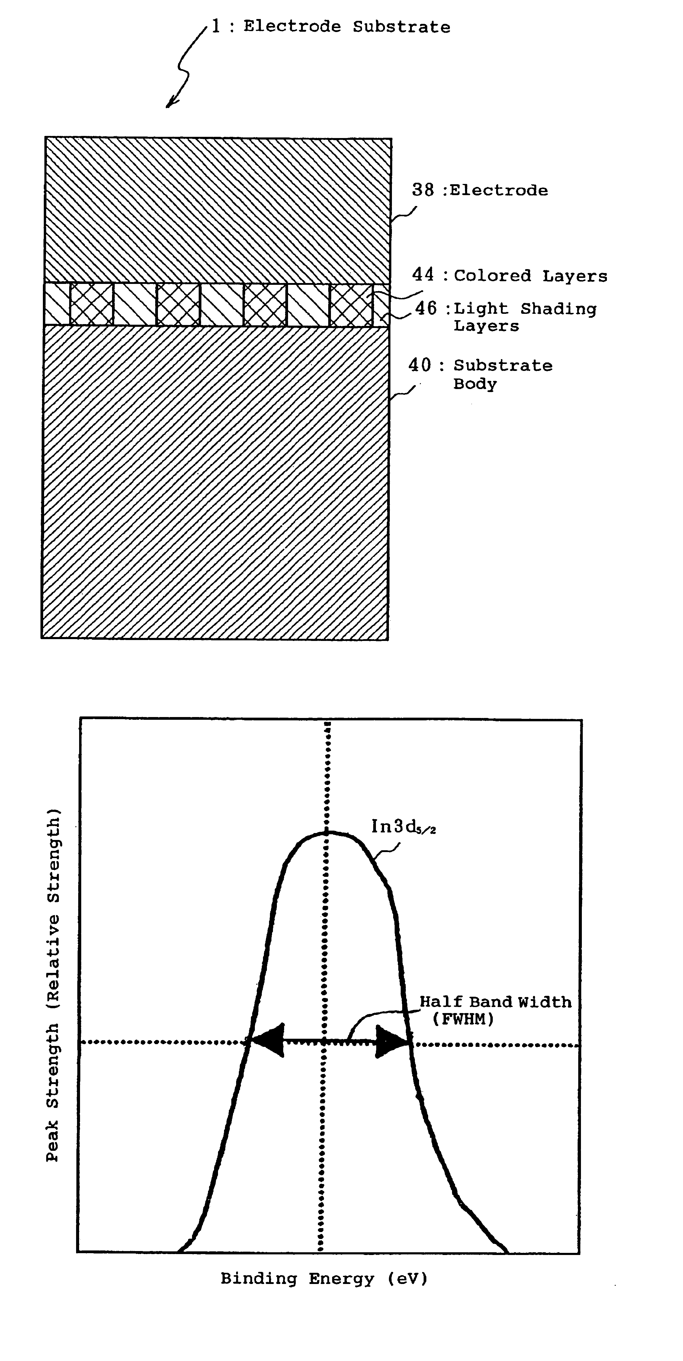
[0066]A first embodiment provides an electrode substrate comprising an electrode substrate comprising a compound containing an In atom and a substrate body wherein the ratio of the half band width [In3d5 / 2]h of an In3d5 / 2 orbit spectral peak measured by X-ray photoelectron spectroscopy (XPS) in the surface of anode to the half band width [In3d5 / 2]n of an In3d5 / 2 orbit spectral peak measured by XPS in the interior of the anode layer, ([In3d5 / 2]h / [In3d5 / 2]n), is from 0.9 to 1.2.
[0067]With reference to drawings, the electrode substrate according to the first embodiment will be concretely explained.
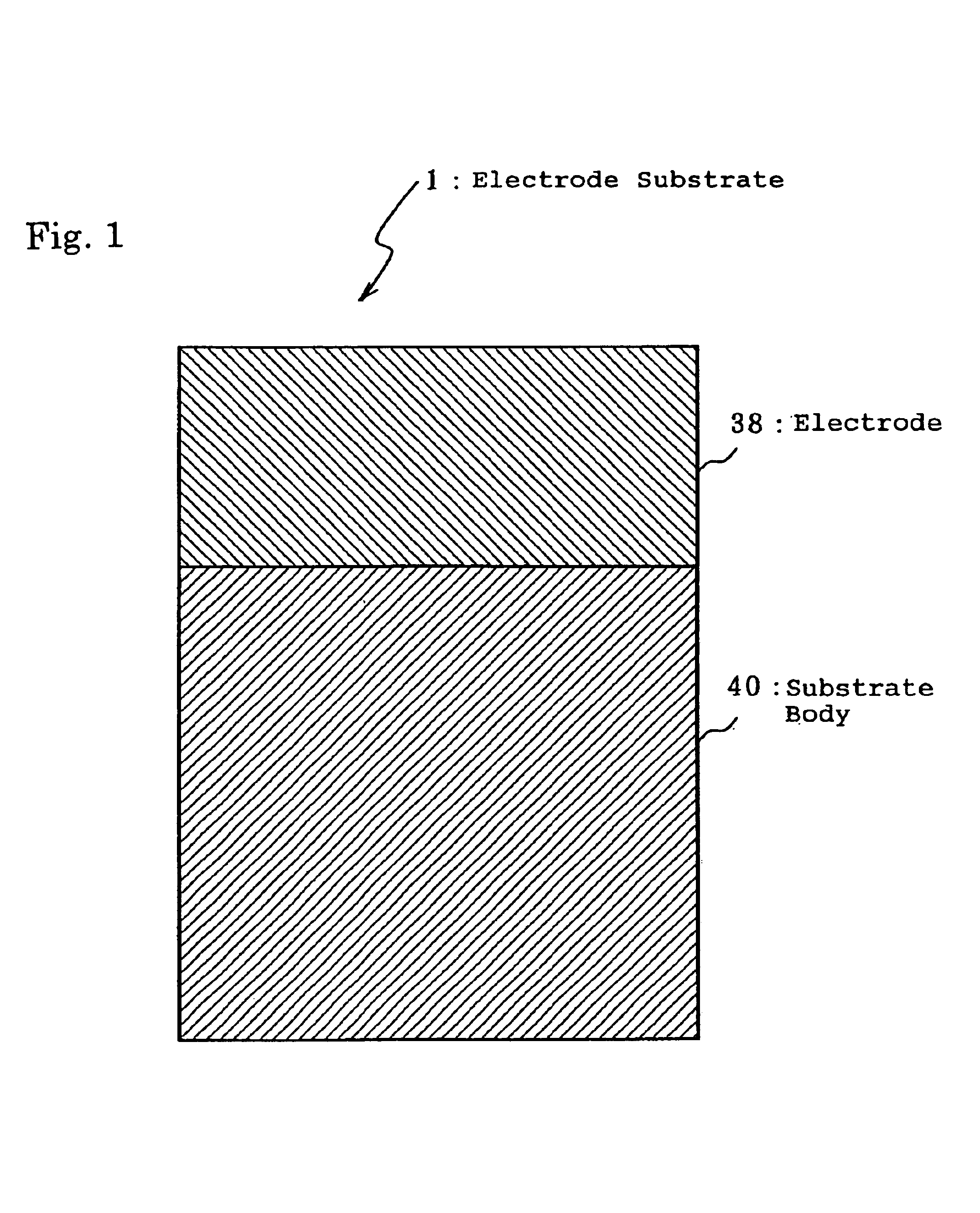
1. Substrate Body
(1) Light Transmittance
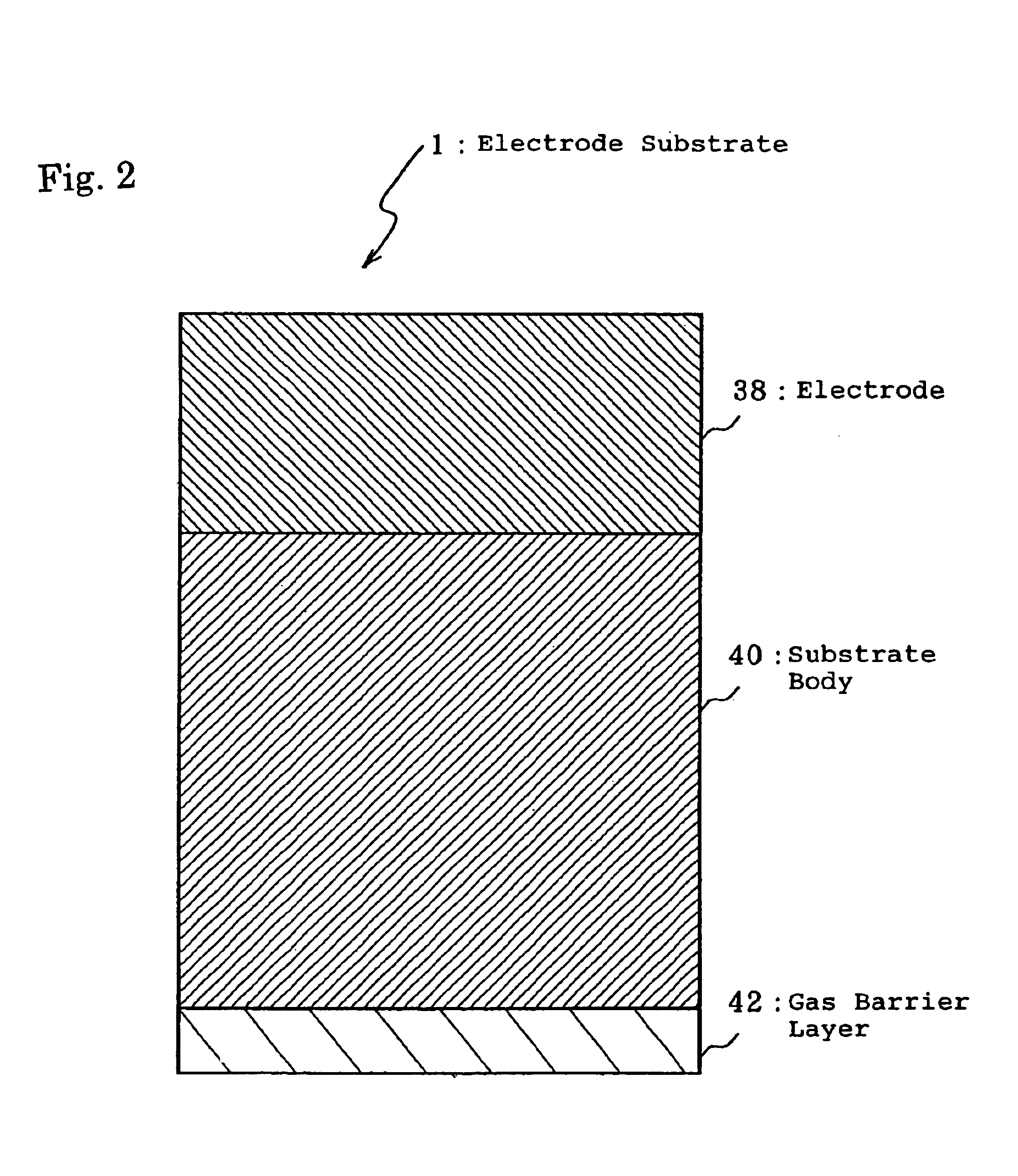
[0068]In an electrode substrate 1 shown in FIG. 1, a substrate body 40 is preferably made of a transparent material, because light transmitted from a transmission liquid-crystal display element, light emitted from an EL element and the like can be effectively taken to the outside.
[0069]Specifically the transparent material preferably h...
second embodiment
[Second Embodiment]
[0180]The second embodiment is directed to a method for producing an electrode substrate, which is characterized by comprising the steps of forming an electrode comprising an indium containing compound on a substrate body, and subjecting the surface of electrode thus formed to inverse sputtering.
[0181]1. Electrode Material Preparation Step (Containing Preparation of Target)
[0182]A target is preferably prepared from an electrode material in advance since a sputtering method can be used for the formation of electrode.
[0183]For the kind and average grain size of material powder, zinc oxide powder with an average grain size of 2 μm or less is preferably used.
[0184]If the average grain size exceeds 2 μm, zinc oxide is liable to diffuse and move for indium oxide and it therefore becomes difficult to control the crystal grain size of hexagonal layered compounds formed. Thus if such a target is used, nodules tend to generate during sputtering.
[0185]Conversely, if the aver...
example 1
(1) Preparation of Substrate with Anode Thereon
[0238]An ITO anode with a thickness of 120 nm was formed on a glass substrate 24 nm long 1.1 mm wide and 1.1 mm thick.
[0239]This electrode substrate was subjected to ultrasonic cleaning while immersed sequentially in isopropyl alcohol, purified water and isopropyl alcohol each for 3 minutes.
[0240]Next a dry nitrogen gas was blown to the glass substrate to remove organic solvents and the like in a clean room of class 1,000. Thereafter the ITO surface was further cleaned using an UV / ozone cleaning machine.
(a) A CeO2 target and a cleaned substrate with ITO (electrode substrate) was placed in a sputtering chamber. The distance from the target to the substrate with ITO was 30 cm.
(b) Next evacuation was carried out. After the evacuated pressure reached to 2×10⁻⁴ Pa or less, 80 sccm of Ar gas was introduced as a discharge gas by a mass flow controller. At this time, the evacuated pressure was 0.38 Pa.
[0241](c) Next while closing a main shutter...
PUM
| Property | Measurement | Unit |
|---|---|---|
| Power | aaaaa | aaaaa |
| Power | aaaaa | aaaaa |
| Magnetic field | aaaaa | aaaaa |
Abstract
Description
Claims
Application Information