
Method and device for waveform shaping of signal light

a waveform and signal light technology, applied in the direction of optical resonator shape and construction, instruments, optical elements, etc., can solve the problems of signal-to-noise ratio, transmission limit, transmission distance limit, etc., and achieve the effect of sufficient optical 3r functions

Inactive Publication Date: 2005-11-08
FUJITSU LTD
View PDF18 Cites 19 Cited by
  • Summary
  • Abstract
  • Description
  • Claims
  • Application Information

AI Technical Summary

Benefits of technology

[0016]It is therefore an object of the present invention to provide a method and device for waveform shaping which can obtain sufficient optical 3R functions.
[0020]According to the present invention, it is possible to suppress amplitude noise or the like generated in the optical AND circuit due to the jitter or temporal instability of the optical signal and the clock pulses. Accordingly, optical signal processing such as optical 3R processing, wavelength conversion processing, and optical demultiplexing processing can be stably performed also to an ultrafast signal. Thus, the object of the present invention can be achieved.

Problems solved by technology

In this kind of optical amplifier, amplified spontaneous emission (ASE) noise generated in association with the amplification is added to cause a reduction in signal-to-noise ratio (S / N ratio), so that the number of repeaters is limited to result in the limit of a transmission distance.
Further, waveform degradation due to the chromatic dispersion owned by an optical fiber and the nonlinear optical effects in the fiber is another cause of the transmission limit.
However, since the performance of this device depends on the operating speed of electronics, it is difficult to operate the O-E-O conversion type device at 40 Gb / s or more.
On the other hand, the all-optical type device has not yet reached a practical level, but some methods have been proposed.
The waveform shaping device for providing the optical 3R functions has a problem that sufficient 3R functions cannot be obtained in some case according to a relative temporal deviation between the optical signal and the regenerated optical clock pulses input into the optical AND circuit.
Such a relative temporal deviation may be caused by the walk-off between the optical signal and the regenerated optical clock pulses in the optical AND circuit or the temporal instability and jitter of each optical pulse, for example.

Method used


Image

  • Method and device for waveform shaping of signal light
  • Method and device for waveform shaping of signal light
  • Method and device for waveform shaping of signal light

Examples


Embodiment Construction

[0028]Preferred embodiments of the present invention will now be described in detail with reference to the attached drawings. Throughout the drawings, substantially the same or like parts are denoted by the same reference numerals.

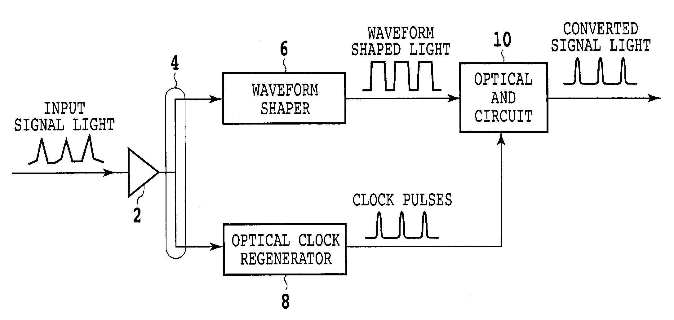
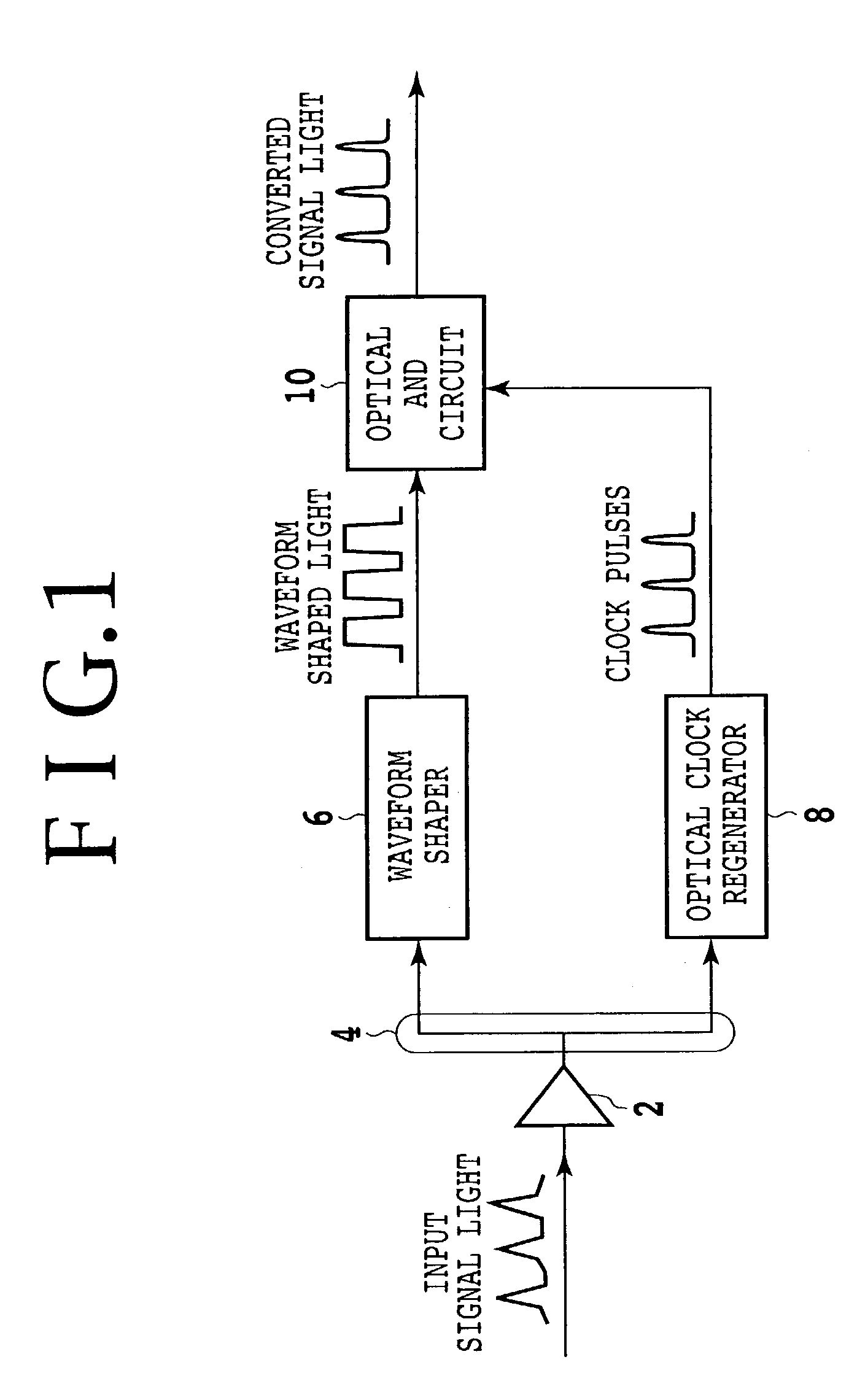
[0029]FIG. 1 is a block diagram showing a first preferred embodiment of the device according to the present invention. This device includes an optical amplifier 2, an optical coupler 4, a waveform shaper 6, an optical clock regenerator 8, and an optical AND circuit 10.

[0030]An optical signal (input signal light) to be waveform shaped is amplified by the optical amplifier 2, and next split into first and second optical signals by the optical coupler 4. The first optical signal is supplied to the waveform shaper 6. In the waveform shaper 6, the pulse widths of the first optical signal are increased to obtain waveform shaped light. The waveform shaped light thus obtained is output from the waveform shaper 6. On the other hand, the second optical signal is sup...


PUM


Abstract

The method according to the present invention includes the steps of splitting an optical signal into first and second optical signals, increasing the pulse widths of the first optical signal to obtain waveform shaped light, generating clock pulses according to the second optical signal, and inputting the waveform shaped light and the clock pulses into an optical AND circuit 10 to obtain a converted optical signal. According to the present invention, it is possible to suppress amplitude noise or the like generated in the optical AND circuit due to the jitter or temporal instability of the optical signal and the clock pulses.

Description

BACKGROUND OF THE INVENTION[0001]1. Field of the Invention[0002]The present invention relates to a method and device for waveform shaping of signal light.[0003]2. Description of the Related Art[0004]In an optical fiber communication system that has been put to practical use in recent years, a reduction in signal power due to transmission line loss, coupling loss, etc. is compensated by using an optical amplifier such as an erbium doped fiber amplifier (EDFA). The optical amplifier is an analog amplifier, which functions to linearly amplify a signal. In this kind of optical amplifier, amplified spontaneous emission (ASE) noise generated in association with the amplification is added to cause a reduction in signal-to-noise ratio (S / N ratio), so that the number of repeaters is limited to result in the limit of a transmission distance. Further, waveform degradation due to the chromatic dispersion owned by an optical fiber and the nonlinear optical effects in the fiber is another cause o...

Claims


Application Information

Patent Timeline
IPC IPC(8): H04B10/17G02F1/35G02F1/365H01S3/06H01S3/067H01S3/10H01S3/108H04B10/2507H04B10/556
CPCH04B10/299
Inventor WATANABE, SHIGEKIFUTAMI, FUMIO
Owner FUJITSU LTD
Learn More