Apparatus and method for disturb-free programming of passive element memory cells

a memory cell and passive element technology, applied in electrical apparatus, digital storage, instruments, etc., can solve the problems of increasing voltage stress which can erroneously write adjacent bits, and unintentional programming of adjacent memory cells, so as to increase processing steps and manufacturing costs

Inactive Publication Date: 2005-11-08
SANDISK TECH LLC
View PDF34 Cites 18 Cited by
  • Summary
  • Abstract
  • Description
  • Claims
  • Application Information

AI Technical Summary

Benefits of technology

[0009]In a passive element memory array, such as a rail stack array having a continuous semiconductor region along one or both of the array lines, we have observed that the programming of a memory cell may cause the unintentional programming of an adjacent memory cell. This is believed to be caused by a leakage path through the continuous semiconductor region from the selected cell to the adjacent cell. In an exemplary antifuse rail stack array, for example, a lightly-doped n-type semiconductor region (i.e., n− region) is continuous along the array line connected to the cathode region of the memory cells. A leakage current through this n− region from a programmed antifuse memory cell to an adjacent unprogrammed memory cell can collapse the depletion region under the adjacent antifuse, causing voltage stress which can erroneously write the adjacent bit. Such an effect may be reduced or eliminated by forming memory cells using a pillar structure rather than a rail stack structure, but this increases processing steps and manufacturing cost.

Problems solved by technology

In a passive element memory array, such as a rail stack array having a continuous semiconductor region along one or both of the array lines, we have observed that the programming of a memory cell may cause the unintentional programming of an adjacent memory cell.
A leakage current through this n− region from a programmed antifuse memory cell to an adjacent unprogrammed memory cell can collapse the depletion region under the adjacent antifuse, causing voltage stress which can erroneously write the adjacent bit.
Such an effect may be reduced or eliminated by forming memory cells using a pillar structure rather than a rail stack structure, but this increases processing steps and manufacturing cost.

Method used


Image

  • Apparatus and method for disturb-free programming of passive element memory cells
  • Apparatus and method for disturb-free programming of passive element memory cells
  • Apparatus and method for disturb-free programming of passive element memory cells

Examples


Embodiment Construction

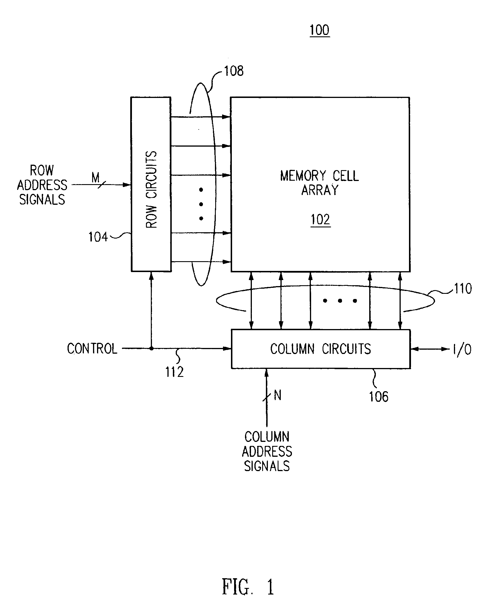
[0025]Referring now to FIG. 1, a block diagram is shown of an integrated circuit 100 including a memory array 102, which diagram may be useful to represent various embodiments of the present invention. In one such embodiment, the memory array 102 is preferably a three-dimensional, field-programmable, non-volatile memory array having more than one level of memory cells. Exemplary three-dimensional memory arrays are disclosed in commonly-assigned U.S. patent application Ser. No. 09 / 560,626 referred to above, and in “Three-Dimensional Memory Array Incorporating Serial Chain Diode Stack” by Kleveland, et al, U.S. patent application Ser. No. 09 / 897,705, filed on Jun. 29, 2001, which is hereby incorporated by reference in its entirety.

[0026]In the presently described embodiment, array 102 is a three-dimensional, non-volatile, write-once memory array of passive element memory cells, although other memory arrays are also suitable. Each passive element memory cell within the memory array 102...


PUM


Abstract

In a passive element memory array, such as a rail stack array having a continuous semiconductor region along one or both of the array lines, programming a memory cell may disturb nearby memory cells as result of a leakage path along the array line from the selected cell to the adjacent cell. This effect may be reduced substantially by changing the relative timing of the programming pulses applied to the array lines for the selected memory cell, even if the voltages are unchanged. In an exemplary three-dimensional antifuse memory array, a positive-going programming pulse applied to the anode region of the memory cell preferably is timed to lie within the time that a more lightly-doped cathode region is pulsed low.

Description

CROSS-REFERENCE TO RELATED APPLICATION(S)[0001]This application is a divisional application of U.S. application Ser. No. 10 / 403,488 by Roy E. Scheuerlein, et al, entitled “Apparatus and Method for Disturb-Free Programming of Passive Element Memory Cells”, filed on Mar. 31, 2003 now U.S. Pat. No. 6,822,903, which application is hereby incorporated by reference in its entirety.[0002]This application is related to co-pending U.S. application Ser. No. 10 / 403,752 by Roy E. Scheuerlein, et al, entitled “Three-Dimensional Memory Device Incorporating Segmented Bit Line Memory Array”, filed on Mar. 31, 2003, which application is hereby incorporated by reference in its entirety.[0003]This application is related to co-pending U.S. application Ser. No. 10 / 403,844 by Roy E. Scheuerlein, et al, entitled “Word Line Arrangement Having Multi-Layer Word Line Segments for Three-Dimensional Memory Array”, filed on Mar. 31, 2003, which application is hereby incorporated by reference in its entirety.FIEL...

Claims


Application Information

Patent Timeline
Patent Type & Authority Patents(United States)
IPC IPC(8): G11C8/00G11C11/34H01L21/336H01L21/02G11C5/00G11C17/16
CPCB82Y10/00G11C13/0014G11C17/16G11C17/165G11C2213/71G11C2213/72
Inventor SCHEUERLEIN, ROY E.KNALL, N. JOHAN
Owner SANDISK TECH LLC
Why Eureka
Try Eureka