Eureka AIR delivers breakthrough ideas for toughest innovation challenges, trusted by R&D personnel around the world.

Magnetoresistive random access memory with reduced switching field variation

a random access memory and switching field technology, applied in the field of magnetic memory devices, can solve the problems of high density of dram, high read and write speed, volatile and large cell area

Inactive Publication Date: 2005-11-22
EVERSPIN TECHNOLOGIES
View PDF313 Cites 16 Cited by
  • Summary
  • Abstract
  • Description
  • Claims
  • Application Information

AI Technical Summary

Problems solved by technology

SRAM has fast read and write speeds, but it is volatile and requires large cell area.
DRAM has high density, but it is also volatile and requires a refresh of the storage capacitor every few milliseconds.
This requirement increases the complexity of the control electronics.
Drawbacks to FLASH include high voltage requirements and slow program and erase times. Also, FLASH memory has a poor write endurance of 104–106 cycles before memory failure.
In addition, to maintain reasonable data retention, the thickness of the gate oxide has to stay above the threshold that allows electron tunneling, thus restricting FLASH's scaling trends.

Method used

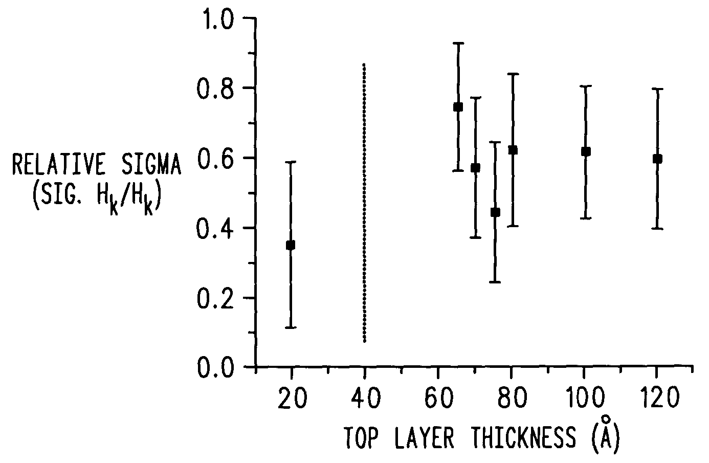
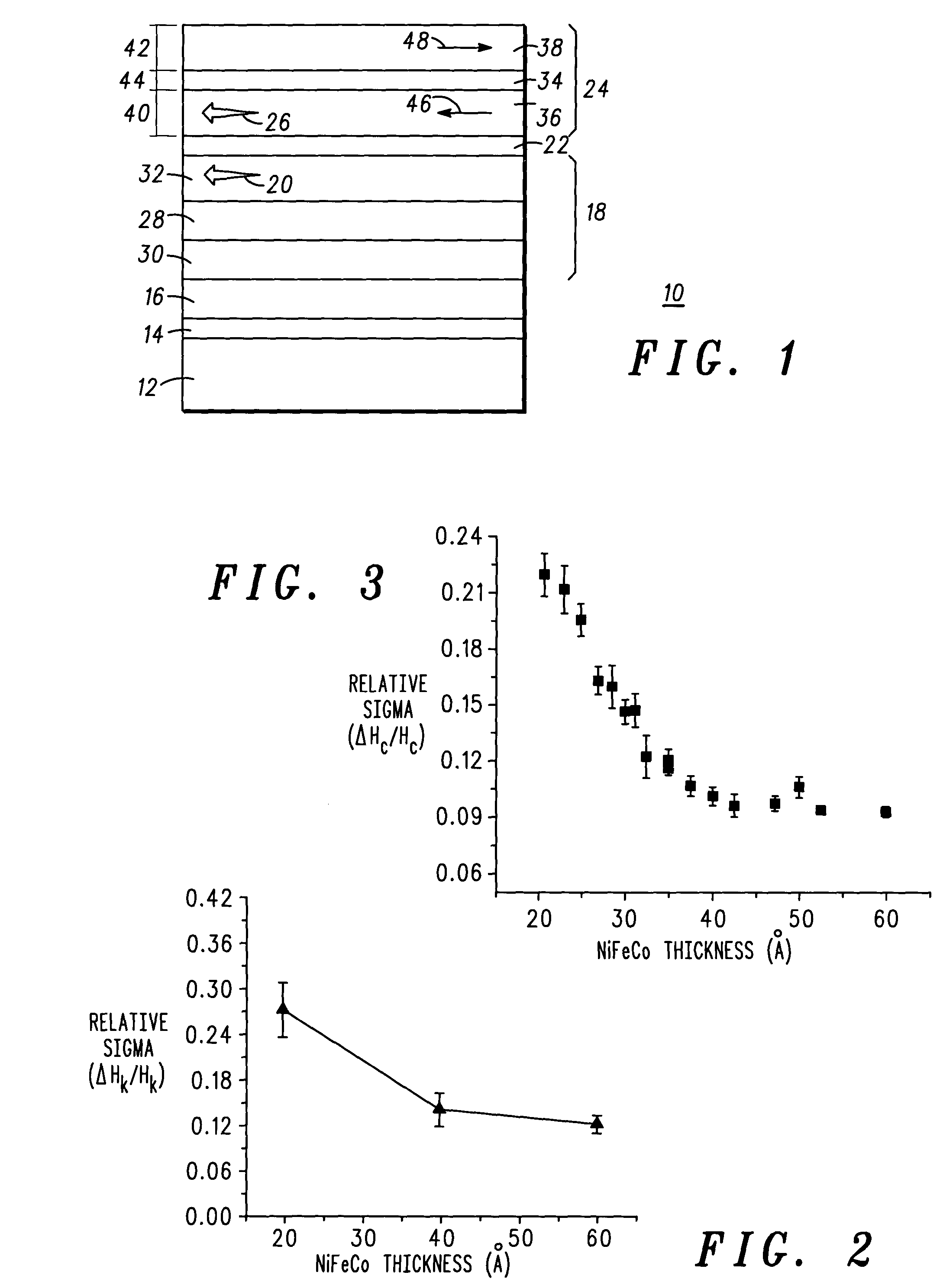
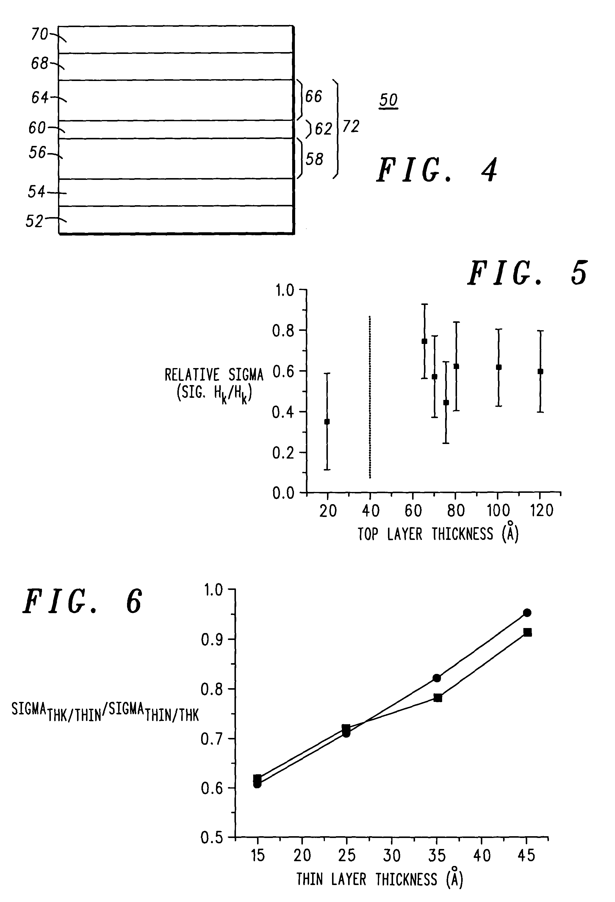

Image

  • Magnetoresistive random access memory with reduced switching field variation
  • Magnetoresistive random access memory with reduced switching field variation
  • Magnetoresistive random access memory with reduced switching field variation

Examples


Embodiment Construction

[0013]Turn now to FIG. 1, which illustrates a simplified sectional view of a scalable magnetoresistive tunneling junction memory cell 10 in accordance with the present invention. The scalable magnetoresistive tunneling junction memory cell 10 includes a supporting substrate 12 onto which a seed layer 14 is positioned. Supporting substrate 12 may be, for example, a semiconductor substrate or wafer and semiconductor control devices may then be formed thereon. Seed layer 14 is formed on supporting substrate 12 to aid in the formation and operation of the remaining layers of material. An anti-ferromagnetic layer 16 is then positioned on seed layer 14 and includes, for example, alloys of manganese (Mn) and one of Ni, Fe, Pt, Rh or combinations thereof. It will be understood that seed layer 14 is optional and is included in this preferred embodiment for illustrative purposes. Also, the positioning of anti-ferromagnetic layer 16 is for fabrication convenience with many other possible confi...


PUM

PropertyMeasurementUnit
widthaaaaaaaaaa
aspect ratioaaaaaaaaaa
magneticaaaaaaaaaa

Abstract

An array of multi-state, multi-layer magnetic memory devices (10) wherein each memory device comprises a nonmagnetic spacer region (22) and a free magnetic region (24) positioned adjacent to a surface of the nonmagnetic spacer region, the free magnetic region including a plurality of magnetic layers (36,34,38), wherein the magnetic layer (36) in the plurality of magnetic layers positioned adjacent to the surface of the nonmagnetic spacer region has a thickness substantially greater than a thickness of each of the magnetic layers (34,38) subsequently grown thereon wherein the thickness is chosen to improve the magnetic switching variation so that the magnetic switching field for each memory device in the array of memory devices is more uniform.

Description

FIELD OF THE INVENTION[0001]This invention relates to semiconductor memory devices and, more particularly, to the switching characteristics of an array of multi-layer magnetic memory cells.BACKGROUND OF THE INVENTION[0002]In the past, a variety of magnetic materials and structures have been utilized to form magnetoresistive materials for non-volatile memory elements, read / write heads for disk drives, and other magnetic type applications. Resistance changes due to relative changes in the magnetic states of constituent magnetic regions within these structures allow information to be stored, in the case of memories, or read, in the case of read heads. Memories made of magnetoresistive material, such as Magnetic Random Access Memory (hereinafter referred to as MRAM) has the potential to overcome some of the shortcomings associated within memories currently in production today. Dynamic Random Access Memory (DRAM), Static Random Access Memory (SRAM), and Flash are the three dominant types...

Claims


Application Information

Patent Timeline
Patent Type & Authority Patents(United States)
IPC IPC(8): G11C11/15G11C11/02H01L29/76H01L29/66H01L31/115H01L31/119G11C11/16H01F10/32H01F41/30H01L43/08
CPCB82Y25/00B82Y40/00G11C11/16H01F10/3272H01F41/302H01L43/08H01F10/3254H10N50/10G11C11/15
Inventor JANESKY, JASON A.ENGEL, BRADLEY N.SLAUGHTER, JON M.
Owner EVERSPIN TECHNOLOGIES
Why Eureka
Eureka Blog
Learn More