Phase-locked loop circuit reducing steady state phase error

Active Publication Date: 2005-11-22
RENESAS ELECTRONICS CORP
View PDF6 Cites 10 Cited by
  • Summary
  • Abstract
  • Description
  • Claims
  • Application Information

AI Technical Summary

Benefits of technology

[0019]It is an object of the present invention to provide a PLL circuit which includes an analog PLL circuit that has a

Problems solved by technology

Actually, however, it is very difficult to make the phase difference between the synchronous clock signal (feedback signal) supplied to each of the logic circuits and the reference signal from the external circuit, smaller than a steady state phase error between the reference clock signal supplied to the phase comparator of the analog PLL circuit and the feedback signal due to a relative error or leakage in the circuitry of the analog PLL circuit.
There are limitations on attempts to reduce the steady state phase error due to variations and leakage in the analog PLL circuit, making it difficult to synchronize the synchronous clock signal supplied to each of the logic circuits with the reference clock signal perfectly.
However, if the frequency of the synchronous clock signal is high, then the allowable range for the steady state phase error is so tight that the steady state phase error cannot b

Method used


Image

  • Phase-locked loop circuit reducing steady state phase error
  • Phase-locked loop circuit reducing steady state phase error
  • Phase-locked loop circuit reducing steady state phase error

Examples


Embodiment Construction

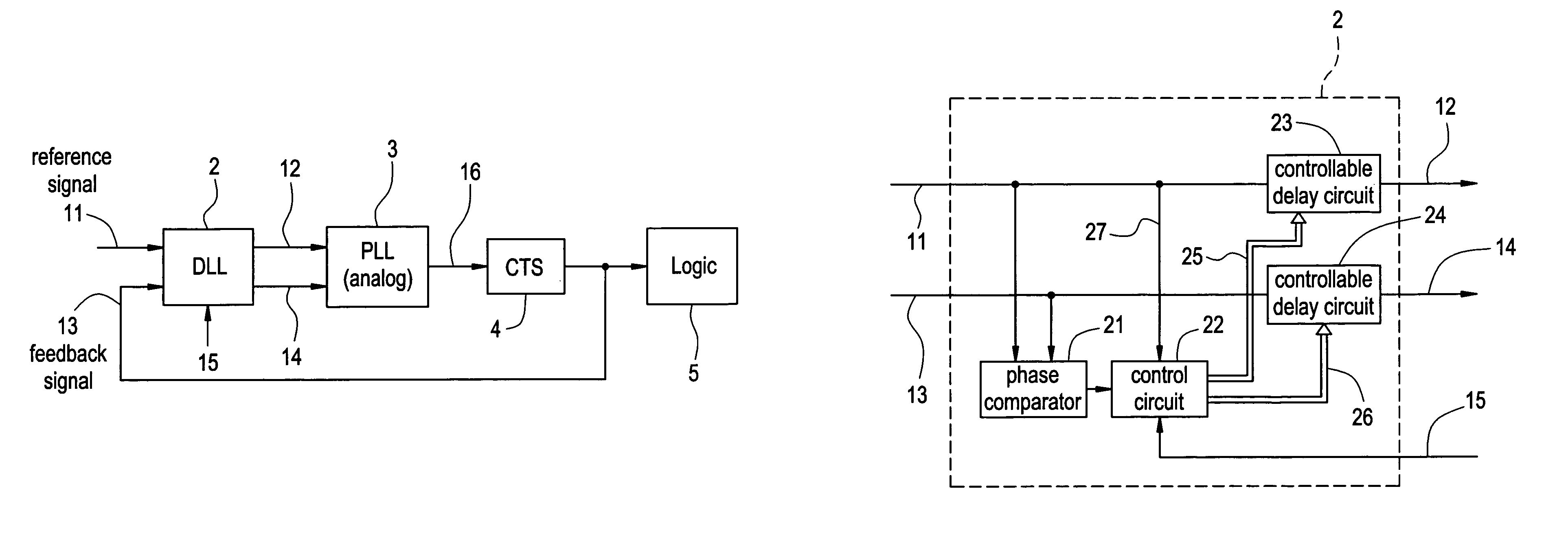
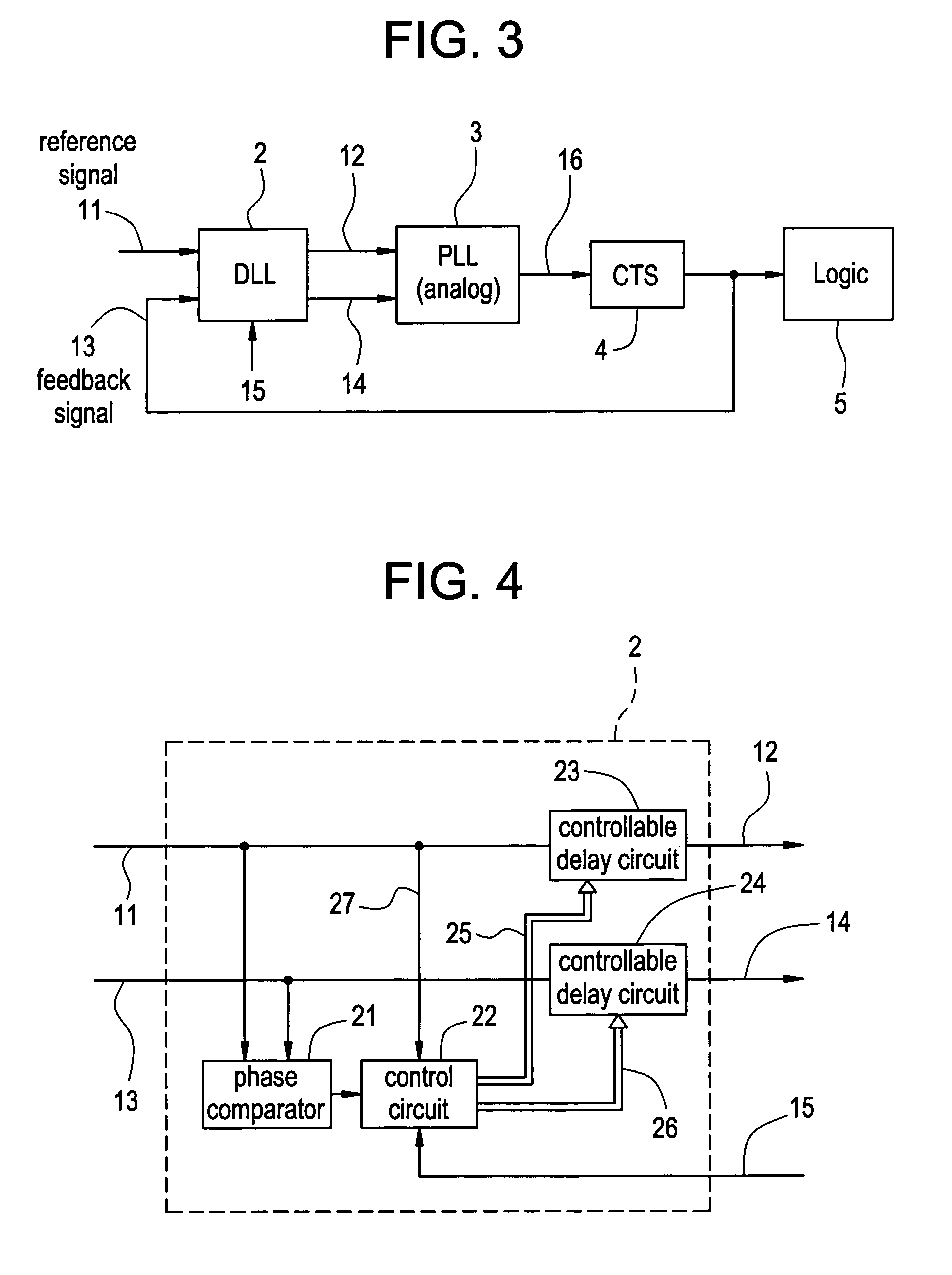
[0032]FIG. 3 shows a block diagram of a PLL circuit according to an embodiment of the present invention. The PLL circuit according to the embodiment of the present invention is incorporated in an integrated circuit chip.

[0033]As shown in FIG. 3, the PLL circuit has internal DLL circuit 2 for comparing the phase of feedback signal 13 as a synchronous clock signal supplied to each of logic circuits 5 in the integrated circuit chip with the phase of reference clock signal 11 supplied from a source external to the integrated circuit chip. If the internal DLL circuit 2 detects a phase difference as a result of the comparison between the phase of feedback signal 13 and the phase of reference clock signal 11, then the internal DLL circuit 2 adds a predetermined phase difference to the detected phase difference to generate reference clock delay signal 12 and feedback delay signal 14, the phase difference therebetween being increased, and supplies reference clock delay signal 12 and feedback...


PUM


Abstract

A phase-locked loop circuit has a DLL circuit in a stage preceding an analog PLL circuit. The DLL circuit detects a phase difference between a reference clock signal and a feedback signal, changes the detected phase difference to a phase difference increased so as to be greater than a steady state phase error which the analog PLL circuit has, and supplies the resultant phase difference to the analog PLL circuit. While the phase difference between the reference clock signal and the feedback signal is being detected by the DLL circuit, the analog PLL circuit operates to reduce the increased phase difference to the steady state phase error. As a result, the phase difference between the reference clock signal and the feedback signal is reduced to a sensitivity limit of a phase comparator in the DLL circuit.

Description

BACKGROUND OF THE INVENTION[0001]1. Field of the Invention[0002]The present invention relates to an analog PLL (Phase-Locked Loop) circuit for use in a semiconductor integrated circuit chip.[0003]2. Description of the Related Art[0004]Semiconductor integrated circuit chips incorporate a PLL circuit for synchronizing a clock signal supplied to various logic circuits in the integrated circuit with a reference clock signal that is supplied from a source external to the integrated circuit.[0005]FIG. 1 of the accompanying drawings shows a block diagram of a conventional PLL circuit in an integrated circuit chip. As shown in FIG. 1, reference clock signal 53 that is supplied from an external source is supplied to an input terminal of analog PLL circuit 52, and a synchronous clock signal supplied to each of logic circuits 57 in an integrated circuit is supplied as feedback signal 54 to another input terminal of analog PLL circuit 52. Analog PLL circuit 52 controls the phase of output clock...

Claims


Application Information

Patent Timeline
IPC IPC(8): H03L7/087H03L7/08H03L7/07H03L7/081
CPCH03L7/07H03L7/081H03L7/087H03L7/08
Inventor HAYASHIDA, KEIJIHASEGAWA, ATSUSHI
Owner RENESAS ELECTRONICS CORP
Why Eureka
Try Eureka