Semiconductor device having an amorphous silicon-germanium gate electrode
a silicon-germanium gate electrode and silicon-germanium technology, applied in the direction of semiconductor devices, radio frequency controlled devices, electrical equipment, etc., can solve the problem of not completely suppressing the permeation of boron atoms
- Summary
- Abstract
- Description
- Claims
- Application Information
AI Technical Summary
Benefits of technology
Problems solved by technology
Method used
Image
Examples
embodiment 1
[0080]Hereinafter, a semiconductor device and a method for fabricating the device in accordance with a first embodiment of the present invention will be described with reference to the accompanying drawings.
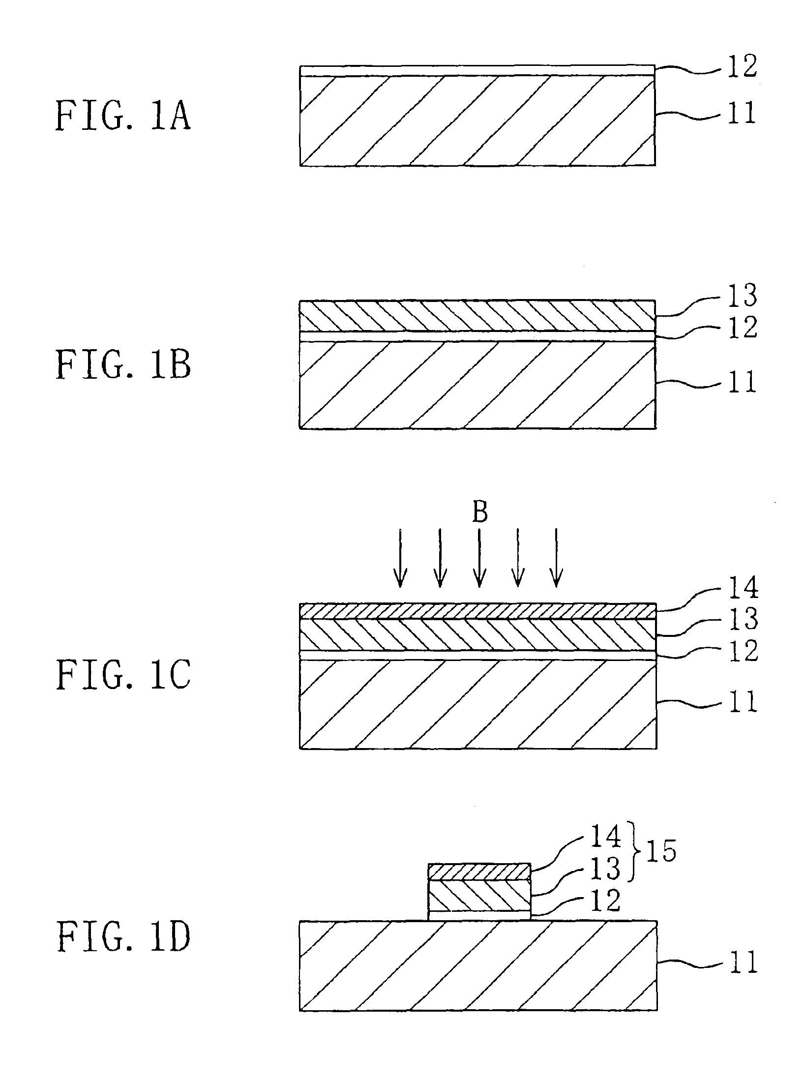
[0081]FIGS. 1A through 1D are cross-sectional views corresponding to respective process steps for fabricating a semiconductor device in accordance with the first embodiment.
[0082]First, as shown in FIG. 1A, a gate insulating film 12 is deposited to a thickness of about 3 nm, for example, on a silicon substrate 11 of a conductivity type.
[0083]Next, as shown in FIG. 1B, a silicon germanium layer 13 (which will be herein called an “SiGe layer”) is deposited to a thickness of 100 nm, for example, on the gate insulating film 12 by an LPCVD (low-pressure chemical vapor deposition) process. In this process, a source gas containing silicon (which will be herein called as an “Si source gas”) and a source gas containing germanium (which will be herein called a “Ge source gas”) are supplied...
modified example of embodiment 1
[0098]Hereinafter, a semiconductor device and a method for fabricating the device in accordance with a modified example of the first embodiment will be described with reference to the accompanying drawings.
[0099]The method of this modified example differs from that of the first embodiment in that the Ge concentration in the SiGe layer 13 is changed in the depth direction by changing the mixture ratio of Si and Ge source gases with time in the process step of depositing the SiGe layer 13 (see FIG. 1B).
[0100]Specifically, the SiGe layer 13 may have a Ge concentration of about 10%, for example, near the lower surface thereof (i.e., part of the SiGe layer 13, close to the interface with the gate insulating film 12) by setting the ratio of the Ge source gas very low or to zero for a while after the SiGe layer 13 started to grow. On the other hand, the SiGe layer 13 may have a Ge concentration of about 70%, for example, near the upper surface thereof by increasing the ratio of the Ge sour...
embodiment 2
[0105]Hereinafter, a semiconductor device and a method for fabricating the device in accordance with a second embodiment of the present invention will be described with reference to the accompanying drawings.
[0106]FIGS. 4A through 4D are cross-sectional views corresponding to respective process steps for fabricating a semiconductor device in accordance with the second embodiment.
[0107]First, as shown in FIG. 4A, a gate insulating film 22 is deposited to a thickness of about 3 nm, for example, on a silicon substrate 21 of a conductivity type. Then, a lower silicon layer 23 (which will be herein called a “lower Si layer”) in an amorphous state is deposited to a thickness of 10 nm, for example, on the gate insulating film 22 by an LPCVD process with an Si source gas such as SiH4 gas supplied at a temperature of about 500° C.
[0108]Next, as shown in FIG. 4B, an SiGe layer 24 is deposited to a thickness of 100 nm, for example, on the lower Si layer 23 by an LPCVD process with Si and Ge so...
PUM
| Property | Measurement | Unit |
|---|---|---|
| thickness | aaaaa | aaaaa |
| thickness | aaaaa | aaaaa |
| temperature | aaaaa | aaaaa |
Abstract
Description
Claims
Application Information


