Optoelectronic devices employing fibers for light collection and emission

Inactive Publication Date: 2005-11-29
KIM II JOHN
View PDF20 Cites 43 Cited by
  • Summary
  • Abstract
  • Description
  • Claims
  • Application Information

AI Technical Summary

Benefits of technology

[0034]The tube may in part have a sinuous form, be supported on a rooftop, be coated with a transparent protective material, be covered with a protective sheet, such as a glass or polymethylmethacrylate shee

Problems solved by technology

The goal of solar energy as an inexpensive, alternative energy source has been a dream for many years, and on occasion that dream seems elusive.
Despite these advances, the prior art fails

Method used


Image

  • Optoelectronic devices employing fibers for light collection and emission
  • Optoelectronic devices employing fibers for light collection and emission
  • Optoelectronic devices employing fibers for light collection and emission

Examples


Embodiment Construction

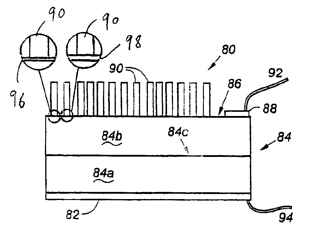
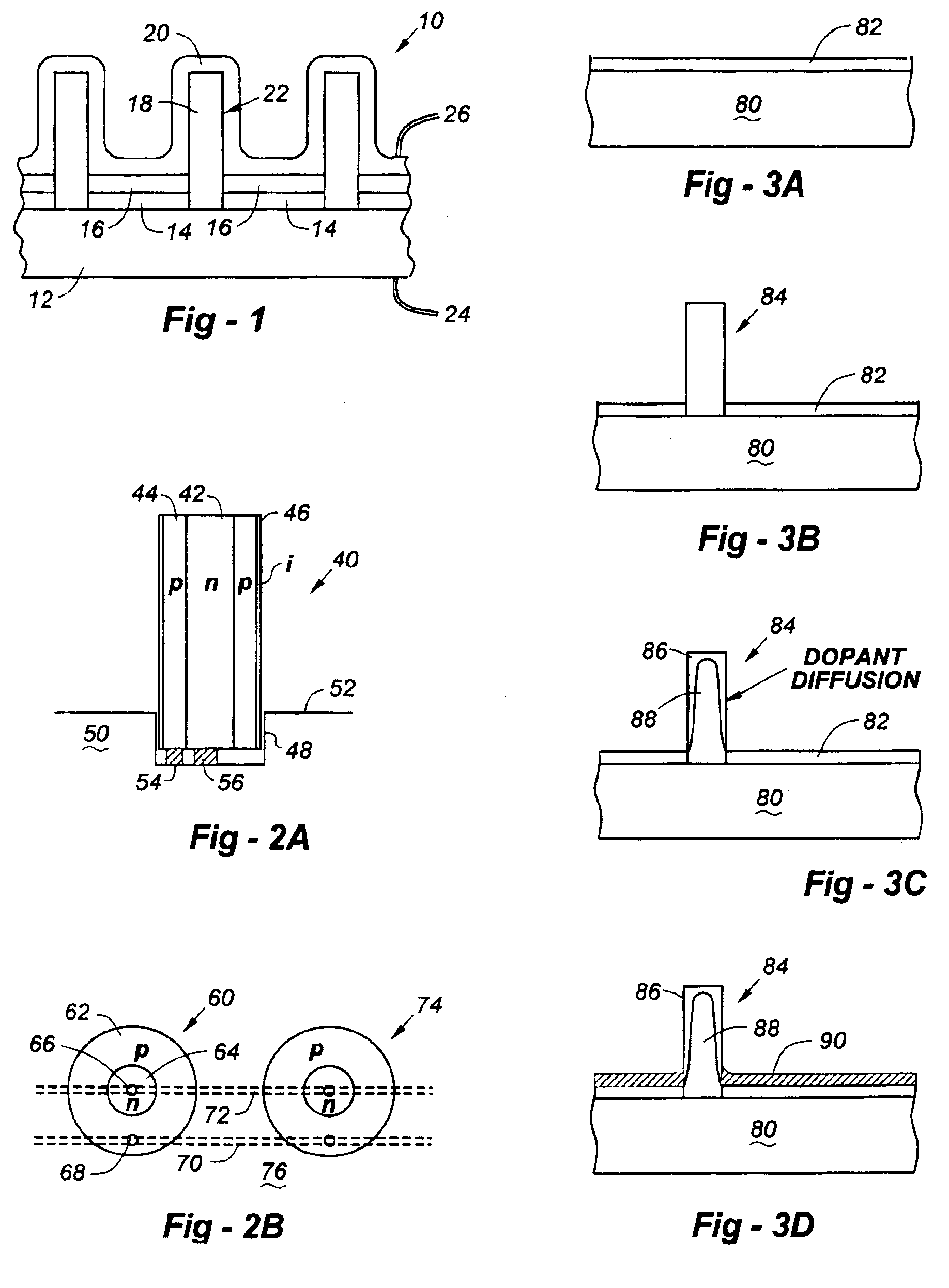
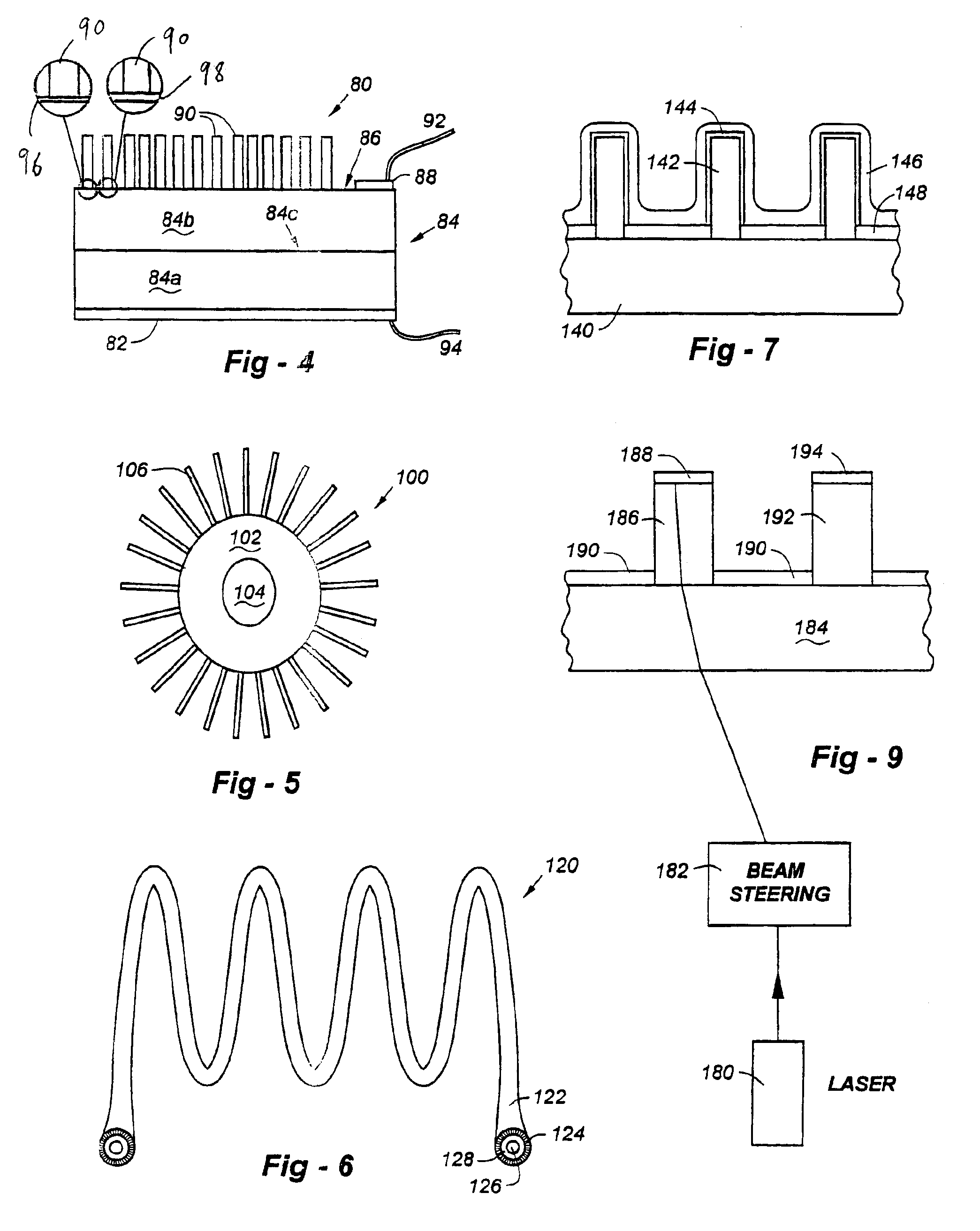
[0058]FIG. 1 shows a cross-section of part of an optoelectronic device, shown generally at 10, comprising an electrically conducting substrate 12, an adhesive layer 14, insulating layer 16. fiber 18, an electrically conducting layer 20, a first electrical contact 24, and a second electrical contact 26.

[0059]The fibers can be deposited on the substrate by a flocking technique, so that adhesive layer 14 is a flock adhesive layer. Flocking techniques are well known in the art, as discussed in more detail later.

[0060]For example, the conducting layer 20 may comprise a p-type doped semiconductor, and the fibers may comprise a n-type doped semiconductor so as to form a p-n semiconductor junction at the interface 22 between the conducting layer and the fiber surfaces. As will be clear to those skilled in the art, the doping pattern can be reversed (i.e. the conducting layer may comprise an p-type doped semiconductor and the fibers comprise an n-type doped semiconductor). It can be advantag...


PUM


Abstract

An optoelectronic device, such as a solar cell, light-emitting device, or photodetector, comprises a substrate, a number of fibers supported by the substrate so that an end of each fiber is in electrical communication with the substrate surface; an optional first layer, covering the substrate, though which the fibers protrude, and a second layer overlaid on at least part of the first layer and exposed fiber surfaces. The second layer may be electrically conducting, and electrically isolated from the substrate surface by the first layer. The second layer can be in electrical communication with each fiber, and an electrically conducting path can exists between the second layer and the substrate surface through each fiber. The substrate, in whole or in part (such as the substrate surface) can be electrically conducting. The electrically conducting path may comprises a semiconductor p-n junction, so that the optoelectronic device emits light, provides a photovoltaic potential, and/or is sensitive to light, for example acting as a photoresistor, photodetector, and the like.

Description

FIELD OF THE INVENTION[0001]The invention relates to improved solar collectors and other devices using one or more substrates supporting a plurality of fibers applied using flocking techniques.BACKGROUND OF THE INVENTION[0002]The goal of solar energy as an inexpensive, alternative energy source has been a dream for many years, and on occasion that dream seems elusive. Various techniques have been attempted and patented to increase efficiency, including multi-bandgap, tandem and compound cells. Experiments have also been tried with respect to physical structures, including concentrators and non-planar collection surfaces.[0003]A search of the prior art was undertaken, and the following references were identified, all of which are incorporated herein by reference:[0004]U.S. Pat. No. 3,780,722 to Swet describes a fiber optical solar receiver, comprising a boule of fibers shaped into an actuate collecting surface at one end.[0005]U.S. Pat. No. 4,117,829 to Gross et al. discloses a heat-...

Claims


Application Information

Patent Timeline
IPC IPC(8): F24S10/70F24S23/00G02B6/04H01L31/0352H01L33/24
CPCF24J2/067H01L31/035281H01L31/03529G02B6/04H01L33/24Y02E10/40Y02E10/50F24S23/12
Inventor KIM, II, JOHN
Owner KIM II JOHN
Why Eureka
Try Eureka