Semiconductor device incorporating internal power supply for compensating for deviation in operating condition and fabrication process conditions

a technology of semiconductor devices and internal power supplies, applied in the direction of logic circuit coupling/interface arrangements, pulse techniques, instruments, etc., can solve the problems of affecting the reliability of the device, unable to avoid remarkable deviations, and unable to accurately count such small (fine) devices or elements and wires, etc., to achieve the effect of improving reliability and high stability

Inactive Publication Date: 2005-11-29
RENESAS TECH CORP
View PDF59 Cites 25 Cited by
  • Summary
  • Abstract
  • Description
  • Claims
  • Application Information

AI Technical Summary

Benefits of technology

[0007]It is therefore an object of the present invention to realize a semiconductor device enjoying high stability and improved reliability by protecting the electrical characteristics and the reliability against changes, notwithstanding a deviation or variation in the condition of the fabrication process condition and the operating condition.
[0009]According to an embodiment of the present invention, the operation voltage and / or operation current of the circuits and / or elements (devices) incorporated in the semiconductor device is controlled in accordance with the electrical characteristics whereby a semiconductor device of high stability and enhanced reliability can be realized.

Problems solved by technology

However, a great difficulty is encountered in fabricating such small (fine) devices or elements and wires accurately, giving rise to a problem that remarkable deviations can not be avoided.
Further, deviations due to the fabrication process condition exert significant influence to the reliability of the device.
More specifically, degradation in the dielectric breakdown strength (dioxide breakdown strength) as well as degradation in the characteristics (due to hot carriers) occur as the result of implementation of the elements in small or minute size.
Further, such characteristics concerning reliability of the device depend by and large on the dispersion in the implemented size.
However, in the prior known techniques mentioned above, no consideration is paid to the influence of the conditions in the fabrication process condition and the operating condition to the electric characteristics and reliability, and thus it has been difficult to realize a semiconductor device of high stability and improved reliability.
Besides, because no consideration is made concerning the influence of the condition in the fabrication process, yield of products of satisfactory quality in a manufacturing on the mass production basis is low, giving rise to a problem that high manufacturing cost is involved.

Method used


Image

  • Semiconductor device incorporating internal power supply for compensating for deviation in operating condition and fabrication process conditions
  • Semiconductor device incorporating internal power supply for compensating for deviation in operating condition and fabrication process conditions
  • Semiconductor device incorporating internal power supply for compensating for deviation in operating condition and fabrication process conditions

Examples


Embodiment Construction

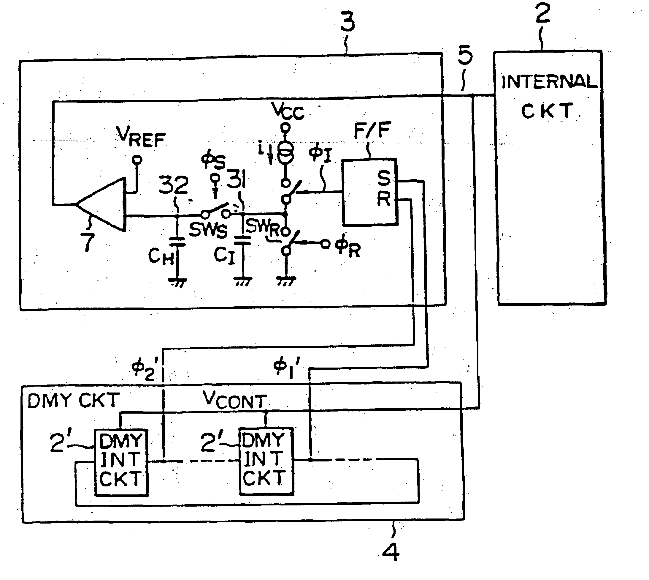
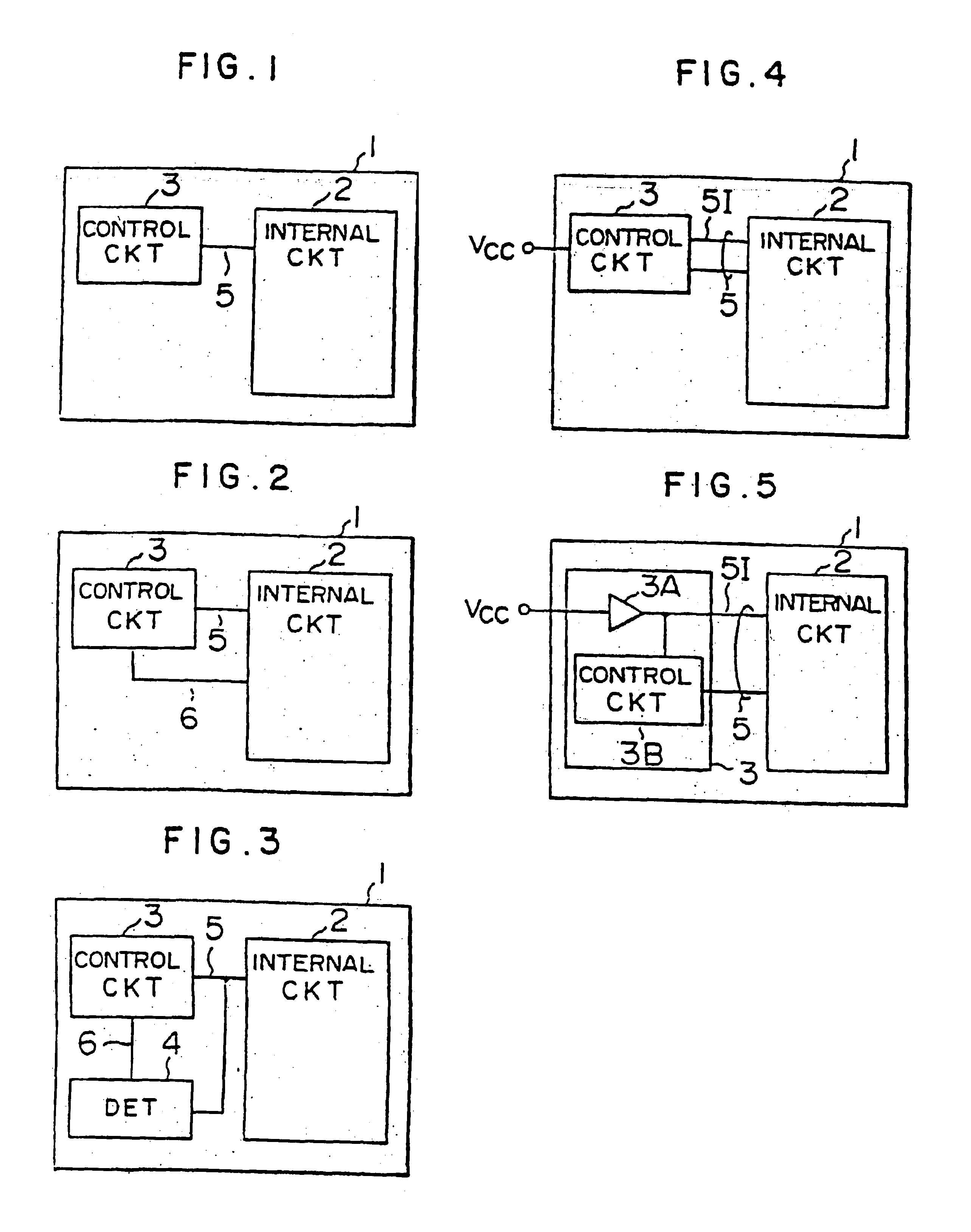
[0014]FIG. 1 is a schematic diagram for illustrating the basic principle underlying an embodiment of the present invention. In this figure, reference numeral 1 denotes a semiconductor chip, 2 denotes an internal circuit inherent to a semiconductor device, and a numeral 3 denotes a control circuit implemented according to the invention for generating control signals or controlled internal voltages in accordance a deviation in the condition in the fabrication process as well as the operating condition in which the semiconductor device is used. The control signal or internal voltage as generated is utilized for controlling operation of the internal circuit 2 by way of a control bus or line 5. Although a single line 5 is shown, it will be readily understood that a number of signal lines may be prepared in the form of a bus in conformance with the configuration of the internal circuit 2.

[0015]According to the illustrated embodiment of the invention, the characteristics of the internal ci...


PUM


Abstract

A semiconductor integrated circuit comprises a semiconductor chip, a power supply terminal provided on the semiconductor chip for receiving a voltage from an external power supply source, an internal circuit provided on the semiconductor chip, a power supply circuit provided on the semiconductor chip for transforming an external power supply voltage received from the power supply terminal for supplying a source voltage resulting from the voltage transformation to the internal circuit, and a control circuit provided on the semiconductor chip for controlling the power supply circuit, wherein the control circuit includes external power supply voltage detecting means and / or temperature detecting means and responds to the signal from the external power supply voltage detecting means and / or the temperature detecting means by changing the power supply voltage to the internal circuit to thereby maintain the operating speed of the internal circuit to be constant.

Description

CROSS REFERENCES TO RELATED APPLICATIONS[0001]This application is a division of application Ser. No. 10 / 103,827 filed 25 Mar. 2002 now U.S. Pat. No. 6,608,791, which is a continuation of application Ser. No. 09 / 506,438 filed on Feb. 18, 2000, now U.S. Pat. No. 6,363,029, which is a continuation of application Ser. No. 08 / 305,528 filed 13 Sep. 1994, U.S. Pat. No. 5,822,267, which is a continuation of application Ser. No. 07 / 985,076 filed on 3 Dec. 1992, U.S. Pat. No. 5,377,156, which is a division of application Ser. No. 07 / 808,878 filed on 18 Dec. 1991, U.S. Pat. No. 5,197,033, which is a division of application Ser. No. 07 / 608,640 filed on 5 Nov. 1990, U.S. Pat. No. 5,086,238, which is a continuation of application Ser. No. 07 / 196,743 filed on 20 May 1988, abandoned, which is a continuation-in-part of: a) application Ser. No. 07 / 126,485 filed on 30 Nov. 1987, U.S. Pat. No. 4,873,673; and b) application Ser. No. 07 / 130,640 filed on 9 Dec. 1987, U.S. Pat. No. 4,837,462, which in turn...

Claims


Application Information

Patent Timeline
Patent Type & Authority Patents(United States)
IPC IPC(8): G11C5/14G11C7/00G11C7/12G11C8/00G11C8/10G11C11/4094H03K5/08H03K17/00H03K17/693H03K19/003H03K19/017H03K19/0175H03K19/0944
CPCG11C5/14G11C5/147G11C7/12G11C8/10G11C11/4094G11C11/413H03K5/08H03K17/693H03K19/00376H03K19/00384H03K19/017H03K19/01707H03K19/017518H03K19/09448H03K2217/0036
Inventor WATANABE, TAKAOHORI, RYOICHIKITSUKAWA, GOROKAWAJIRI, YOSHIKIKAWAHARA, TAKAYUKIITOH, KIYOO
Owner RENESAS TECH CORP
Why Eureka
Try Eureka