Method, apparatus and computer program product for high speed memory testing

a memory and high-speed technology, applied in the direction of resistance/reactance/impedence, testing circuits, instruments, etc., can solve the problems of synchronizing all the cards, limiting the patterns of alu, and not being able to generate patterns without substantial constraints

Inactive Publication Date: 2005-11-29
IBM CORP
View PDF9 Cites 23 Cited by
  • Summary
  • Abstract
  • Description
  • Claims
  • Application Information

AI Technical Summary

Benefits of technology

[0016]The foregoing need is addressed in the present invention. A process of the present invention (referred to herein as a pin vector generator or a bit vector generator) strips out patterns for each individual DUT signal pin (address pin, data pin, etc.) from conventional full-width test vectors. These full-width test vectors are from test patterns produced by a conventional test program. (They are referred to as full-width test vectors because they have widths equal to the whole address and data field width of the DUT.) The slicing of the conventional full-width test vectors by the pin generator produces a pin vector for each one of the DUT pins. The pin vectors are compressed and packaged to produce packets of data which are saved in a suitable storage media before test. Each packet also includes the address of its target channel card as well as one or more pointers to relevant timing and voltage data, such data being referred to herein as DUT vectors. This preprocessing of test vectors avoid the necessity of high-speed, on-the-fly, test pattern generation via hardware ALUs during test. This also removes limitations on the types of test patterns that can be generated.
[0021]A few high speed optical control signals are transmitted on the optical bus and converted by a converter into electrical signals. The electrical signals are then divided by dividers to produce secondary electrical clocks clk0, clk1 . . . clkx at each of the channel cards. This mechanism advantageously produces all the necessary high speed electrical signals only very close to the DUT. Also, a high frequency reference clock is delivered in the optical domain in this manner, which provides critical high speed synchronism and control of timing signals needed for high speed testing. This avoids the necessity of the difficult task of delivering high speed electrical signals from the main frame to the channel cards in the test head. Using the optical signal to synchronize the channel cards also reduces constraints commonly associated with high speed synchronization in the electrical domain over a long transmission line and with large loads such as a large number of channel cards.
[0022]To restate the above, the tester of the present invention advantageously utilizes distributed operations (distributed both in software and in hardware domains) to replace functions of conventional ALU's and utilizes a wider but slower electrical data bus and a narrow but much faster optical control bus. The buses of the present invention traverse only a very short path between the parallel-in serial-out high speed buffer in the test head and the DUT for critical high speed operations. Thus, according to the invention, preprocessed pin vectors are transmitted over the data bus at a frequency that is substantially lower than the testing frequency of the DUT. (This is in contrast to the conventional practice of using hardware ALU's to generate address and data patterns at test speed on-the-fly and transmitting the patterns at high speed.) This, in turn, enables the present system to be used to test devices that operate at higher frequencies than would otherwise be possible and enables the use of a software program written in a high-level language, such as Perl, Java, etc., running on a conventional computer to generate the pin vectors, instead using of special, dedicated and localized high-speed hardware ALU's. This also permits flexibility regarding the patterns that can be generated for the pin vectors.
[0024]In an alternative embodiment an optical bus is provided for data transmission instead of the previously mentioned electrical data bus. This increases the maximum achievable testing frequency and can also support testing of devices with higher signal pin counts, i.e., devices needing more channel cards.

Problems solved by technology

However, the patterns are all limited by the constraints of the ALU architecture.
That is, although such an ALU is programmable, the patterns that the ALU can generate still are not without substantial constraints because the ALU is designed for a certain limited set of op codes.
However, there is still a problem of synchronizing all the cards 131, which may number even in the hundreds.
This is a considerable problem at high speed.
Moreover, the problem of flexibility in pattern generation still exists.
Both of these conventional features limit tester functionality at high speed because with this arrangement write and read operations of the tester are highly critical all the way from the main frame to the DUT and back.
Also, as mentioned before, the hardware ALU's, due to their architectural limitations, can only generate certain types of test patterns.

Method used


Image

  • Method, apparatus and computer program product for high speed memory testing
  • Method, apparatus and computer program product for high speed memory testing
  • Method, apparatus and computer program product for high speed memory testing

Examples


Embodiment Construction

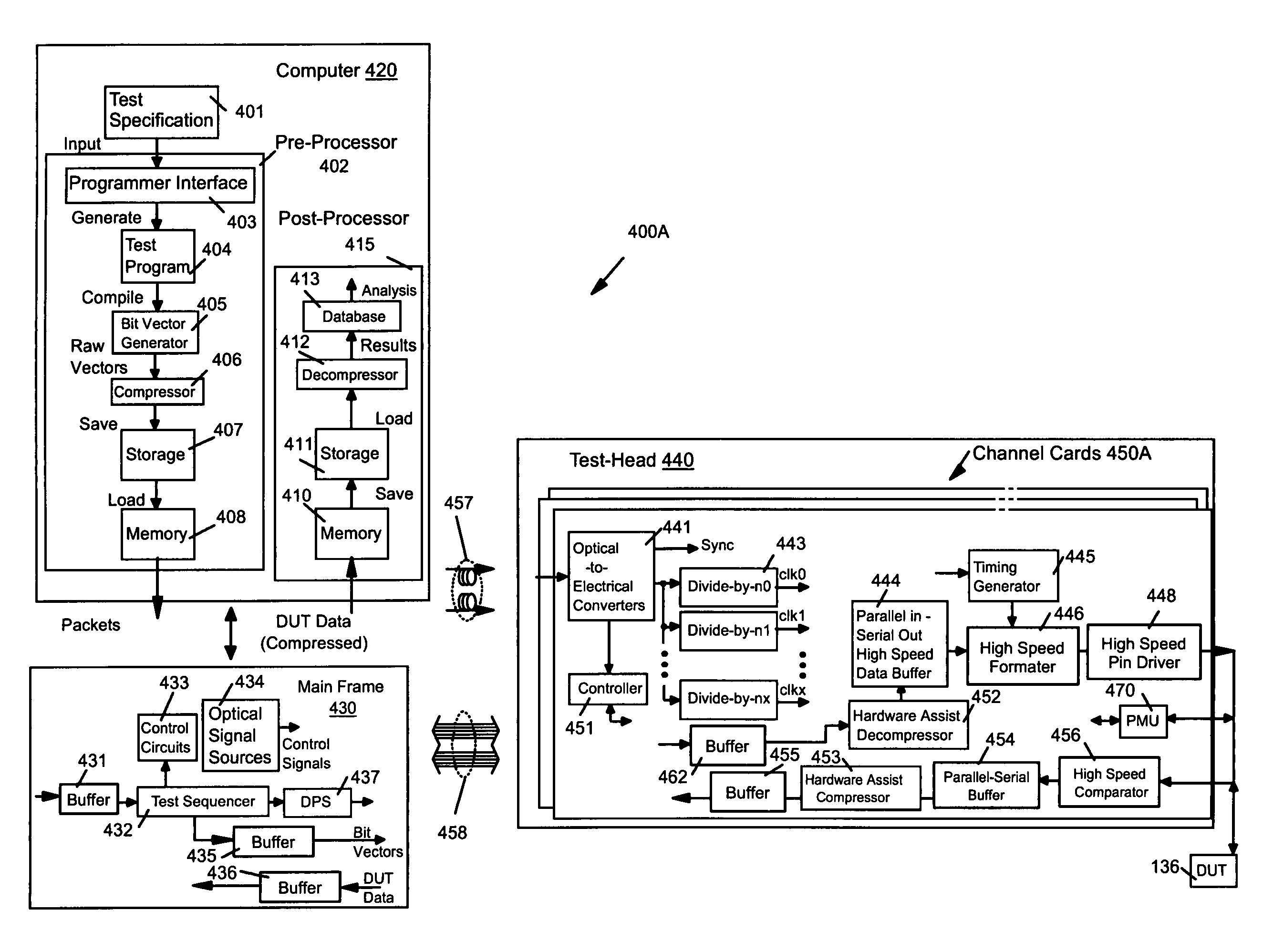
[0043]The claims at the end of this application set out novel features which applicants believe are characteristic of the invention. The invention, a preferred mode of use, further objectives and advantages, will best be understood by reference to the following detailed description of an illustrative embodiment read in conjunction with the accompanying drawings.

[0044]Referring now to FIG. 4A, test system 400A is illustrated in block diagram form, according to an embodiment of the present invention. For the illustrated embodiment of the present invention, test packets are produced in computer system 420 by software processes before testing begins. In other words, test packets are “preprocessed” by software block 402. More specifically, test program 404, which receives test specification 401 via programmer interface 403, is converted by a bit vector generator 405 (also referred to herein as a pin vector generator) that has specialized ALU software in a conventional computer system 420...


PUM


Abstract

For testing a device under test (“DUT”) a test specification is converted in a computer system by a pin vector generator process, which includes generating test vectors. The DUT has numerous input pins and such a pin vector is for a signal to drive one such pin. The pin vectors are compressed and saved. Ones of the pin vectors are loaded, upon initialization of a test, into a pipeline having a series of memory stages and extending from the computer system to channel cards in a test head. The pipeline is operated in data transfer cycles, delivering W bits per cycle. The pin vectors are decompressed at the respective channel cards in decompressor read cycles. X bits are read per decompressor cycle, W being greater than X, so that the pipeline may perform its data transfer cycles less frequently than the decompressor performs its read cycles.

Description

BACKGROUND[0001]1. Field of the Invention[0002]The present invention concerns testing of very large scale integrated-circuitry (“VLSI”) devices, and, more particularly, concerns high speed testing of such devices using test patterns.[0003]2. Related Art[0004]Referring now to FIG. 1, a conventional test system 100 is shown for testing very large scale integrated circuitry (“VLSI”) devices, such as memory devices, application specific integrated circuits (“ASIC's”), and microprocessors. The test system 100 (also referred to herein as a “tester”) includes a main frame 120, a test head 130 and a product handler 140. A computer system 110 is used as an interface between an operator and the tester 100. The interface is used to control the tester 100, to load test programs into the main frame 120, to start testing, to collect test results, etc.[0005]Referring now to FIG. 2, details are shown of the test head 130 of the prior art test system 100. The test head 130 includes a housing platfor...

Claims


Application Information

Patent Timeline
Patent Type & Authority Patents(United States)
IPC IPC(8): G06F19/00
CPCG06F11/263G06F11/273
Inventor CAO, TAI ANHNGUYEN, KHANHRAHMAN, AQUILUR
Owner IBM CORP
Why Eureka
Try Eureka