Electronic camera and solid-state camera element that provides a reduced pixel set

a camera element and camera device technology, applied in the field of electronic cameras and solid-state camera devices, can solve the problems of consuming a lot of power, affecting the efficiency of the camera device, and the number of pixels in the camera device and the display element differ, so as to reduce the pixel set, improve the efficiency of the camera device, and improve the effect of speed

Inactive Publication Date: 2005-12-06
JOHNS MANVILLE INT INC +1
View PDF18 Cites 69 Cited by
  • Summary
  • Abstract
  • Description
  • Claims
  • Application Information

AI Technical Summary

Benefits of technology

[0006]The present invention provides a solid-state camera device that can read selected pixels of the pixel matrix to create a reduced pixel set having reduced image data for purposes of image display, or to set photographic conditions. Reading the reduced pixel set can be performed at higher speed and reduced power consumption than prior art devices that read the entire pixel matrix. When it is desired to record the photographic image, the entire pixel matrix may be read for greatest resolution.

Problems solved by technology

However, the number of pixels in the camera device and the display element differ, due to factors such as differences in technical progress between the two types of elements.
Also, in high quality camera devices having many pixels, it is not feasible to use a display element with the same number of pixels because of the high cost of such a display.
This prior art operation, of reading all pixels, storing the image data from all pixels in image memory, and scanning only the required portion of image memory for display has the problems of taking a long time to execute and consuming much power.
In addition, in the case of color picture elements, when image data are systematically selected from image memory, the resulting image may not include all the color signals required for proper color display.

Method used


Image

  • Electronic camera and solid-state camera element that provides a reduced pixel set
  • Electronic camera and solid-state camera element that provides a reduced pixel set
  • Electronic camera and solid-state camera element that provides a reduced pixel set

Examples


Embodiment Construction

)

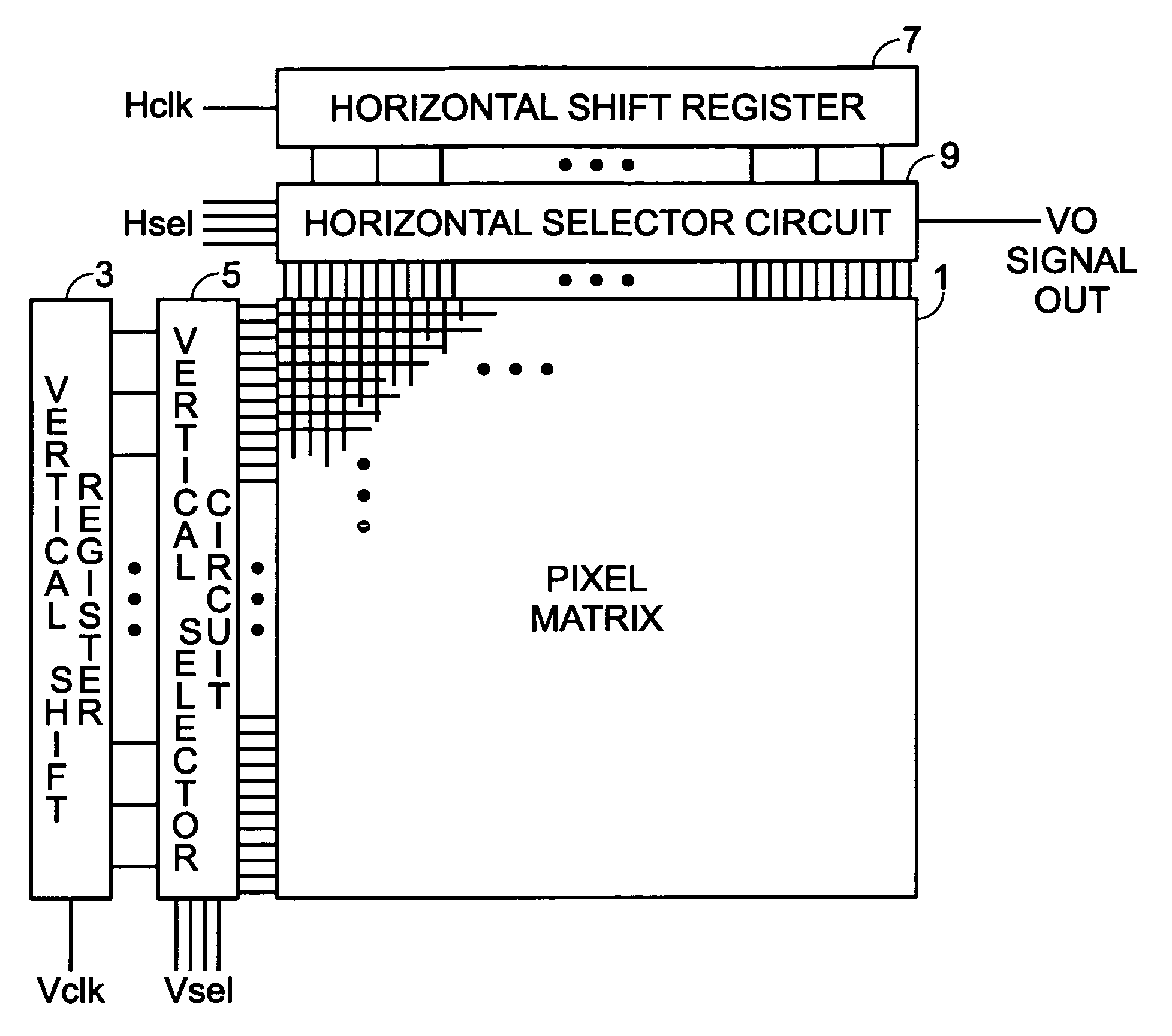
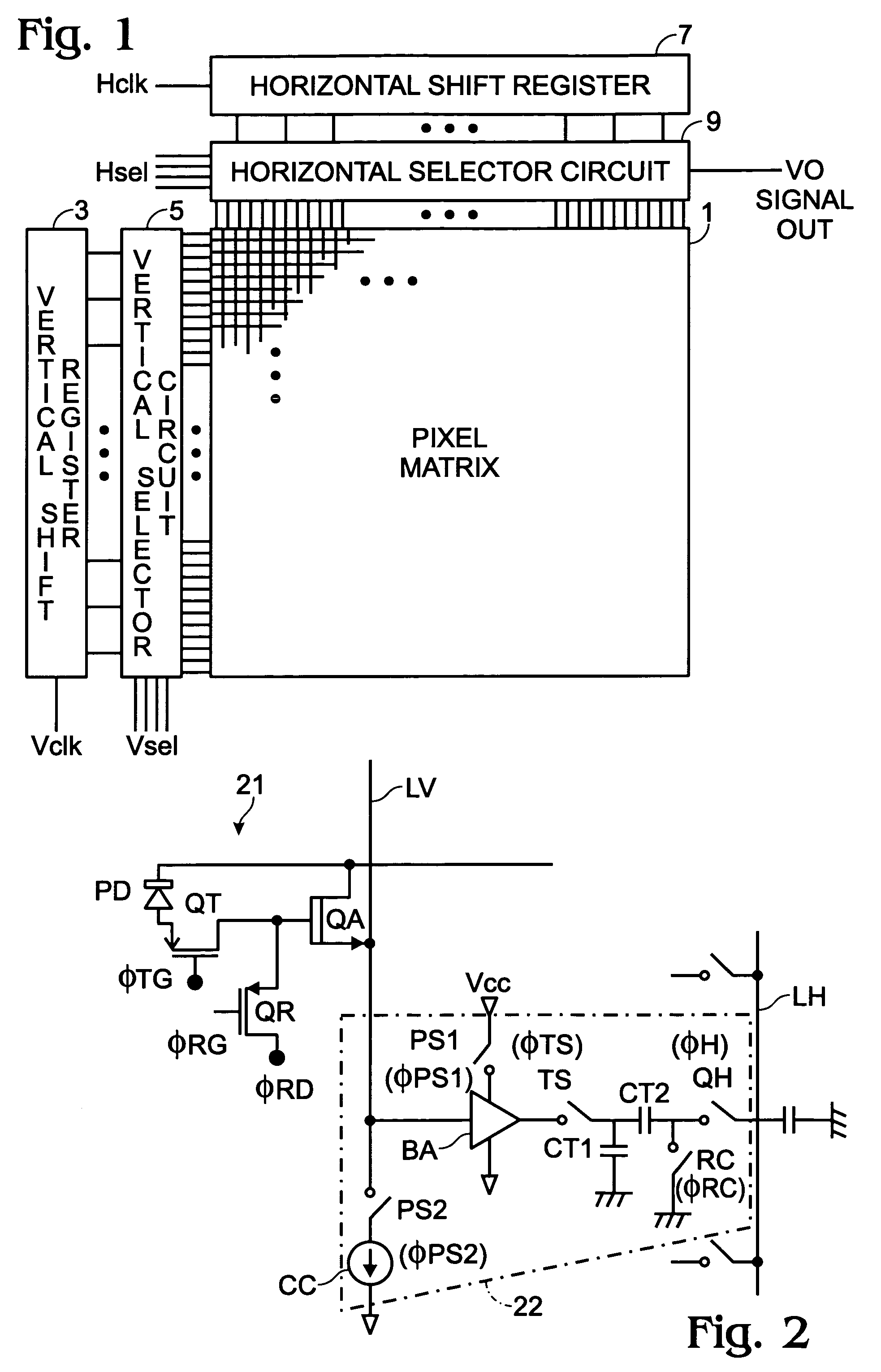
[0026]Before explaining modes of embodiment of this invention, a prior art BCAST system solid-state camera device is explained in summary by reference to FIG. 8. For purposes of explanation, the solid-state camera device of FIG. 8 has four pixels Q(1,1), Q(1,2), Q(2,1), and Q(2,2) arranged in a matrix of two rows and two columns. Each pixel is comprised of photodiode PDij that is a photoelectric conversion element, an amplifier element QAij (comprised, for example, of a junction type field effect transistor (JFET)), a transfer element QTij (exemplarily comprised of a MOSFET) that transfers the charge of the photodiode PD to the gate of amplifier element QAij, and a switch element QRij (exemplarily comprised of a MOSFET) for presetting the gate electrode of amplifier element QAij. The letters i and j correspond to the row and column numbers, respectively.

[0027]In addition, transfer control switch TSj and capacitor CT2j are connected in series between vertical reading line LVj and ho...


PUM


Abstract

A solid-state camera device having a matrix of pixels arranged in rows and columns, wherein a subset of pixels of the entire pixel matrix can be read for display and confirmation of photographic conditions to reduce power consumption and decrease time to display the image. In electronic cameras light is focused on the camera device having pixels and the light energy is used to provide an electric signal from each pixel in proportion to the incident light to provide an image signal. The image signal may be displayed on an attached display such as a liquid crystal display. Because most display have fewer pixels than the camera device, the display can not display image information from each camera device pixel. To thin the number of pixels provided to the display, at least one of a vertical shift register or horizontal shift register includes a selector circuit whereby the respective shift register may select a group of rows or columns, respectively, and the selector circuit can select a single row or column, respectively, from the group. Control signals control the operation of the shift registers and selector circuit(s) and permit selection of desired thinning schemes to optimize the display of image information for best display of colors or minimum energy consumption, as desired.

Description

FIELD OF THE INVENTION[0001]This invention pertains to a solid-state camera device and an electronic camera having the solid-state camera device. More particularly, this invention pertains to reading image information from the solid-state camera device at higher speed and reduced power consumption by reading a subset of pixels of a pixel array to display images or set photographic exposure conditions before recording a photographic image.BACKGROUND OF THE RELATED ART[0002]Electronic cameras focus light through a lens onto a solid-state camera device having light receiving picture elements, or pixels. In charge coupled devices (CCD), these pixels include photodiodes that provide an electrical signal indicative of light incident on the pixel, and other solid-state circuitry to read (that is, transfer) the electrical signal to a display or memory. The pixels are arranged in a matrix of rows and columns. The greater the number and density of pixels in the matrix, the greater the photogr...

Claims


Application Information

Patent Timeline
Patent Type & Authority Patents(United States)
IPC IPC(8): H01L27/146H04N3/14H04N5/232H04N5/235H04N5/335H04N5/345H04N5/369H04N5/374H04N9/07
CPCH04N3/1562H04N5/23241H04N5/23245H04N5/23293H04N23/667H04N25/443H04N25/767H04N25/745
Inventor YOMEYAMA, TOSHIKAZU
Owner JOHNS MANVILLE INT INC
Why Eureka
Try Eureka