Semiconductor device

Inactive Publication Date: 2005-12-13
SEMICON ENERGY LAB CO LTD
View PDF50 Cites 361 Cited by
  • Summary
  • Abstract
  • Description
  • Claims
  • Application Information

AI Technical Summary

Benefits of technology

[0019]The present invention has been made in view of the above problem, and an object of the invention is to provide a semiconductor device (a driving circuit of a display device) which can

Problems solved by technology

Therefore, if there is no third power source having a pote

Method used


Image

  • Semiconductor device
  • Semiconductor device
  • Semiconductor device

Examples


example 1

[0046]In this example, circuits in which a plurality of stages of inverters are connected using the present invention will be described with reference to FIGS. 3A to 3C.

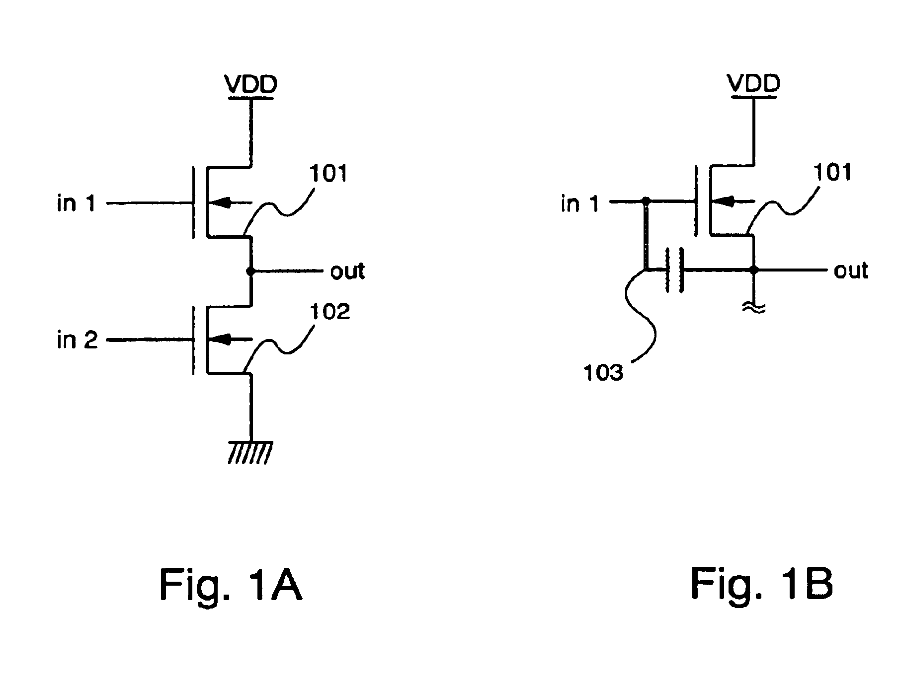
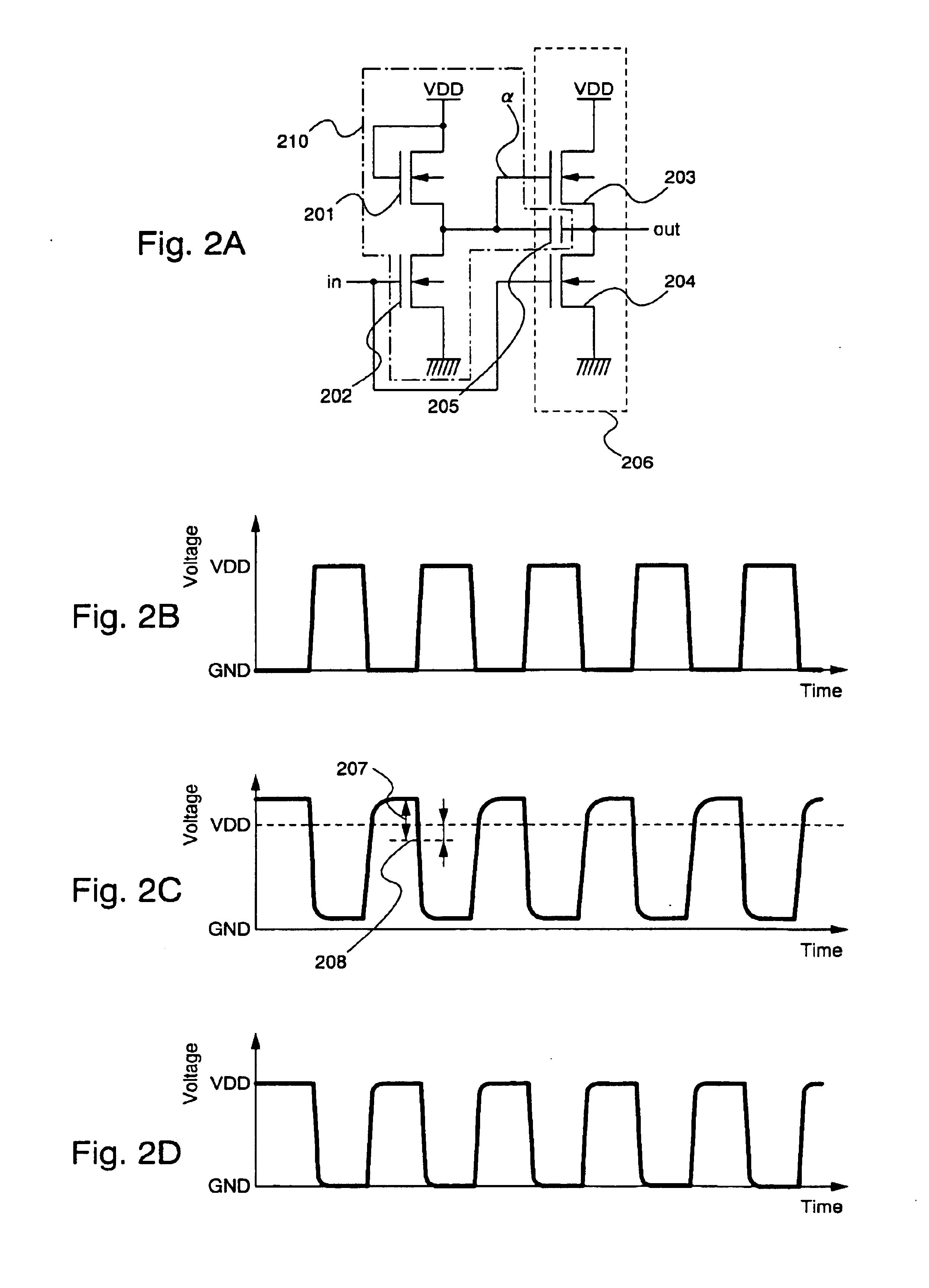
[0047]FIG. 3A shows a circuit in which a plurality of stages of inverters each of which is a mode of a semiconductor device (a driving circuit of a display device) of the present invention are connected. In the driving circuit of the display device or the like, such a circuit is often used as a buffer. In the semiconductor device of the present invention shown in FIG. 3A, manufacturing steps are reduced by using TFTs of only one polarity of either of the N type or the P type, so that it can be fabricated at low cost. Further, an output without amplitude attenuation can be obtained. However, in the case where the circuit as shown in FIG. 3A is employed, the following point should be noted in view of consumed electric power of the circuit.

[0048]In FIG. 3A, when an input signal is at the H level, an N-type TFT 302 is tu...

example 2

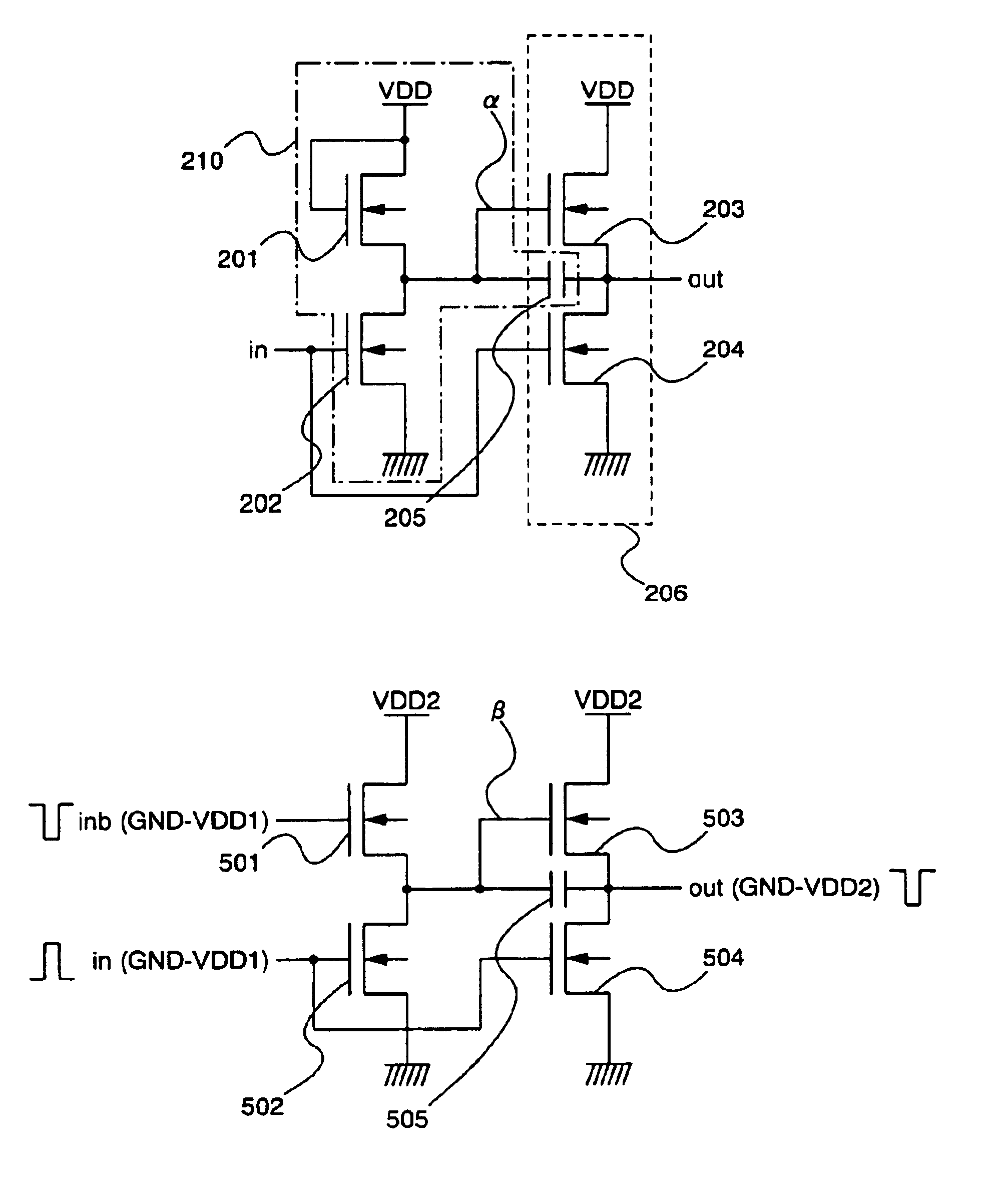
[0053]A semiconductor device (a driving circuit of a display device) of the present invention can easily function as a level shifter by giving a potential which is different from an amplitude potential of an input signal as a power source potential supplied to a circuit. An example will be described below.

[0054]First, as power source potentials, three potentials such as GND, VDD1, and VDD2 are considered, and it is assumed that they have the magnitude relation of GND12. At this time, consideration will be given to a case where a signal having an amplitude of GND-VDD1 is inputted and is converted into a signal having an amplitude of GND-VDD2, and then the signal is extracted.

[0055]FIG. 4A shows an example. The structure of a circuit may be the same as the embodiment and the example 1. The amplitude of an input signal has GND-VDD1, and potentials of power sources connected to ends of impurity regions of N-type TFTs 401 and 403 are referred as VDD2.

[0056]The operation of the circuit wi...

example 3

[0062]In this example, a description will be given on an example in which a display device is fabricated by using a semiconductor device (a driving circuit of a display device) of the present invention.

[0063]FIG. 7 is a schematic view of a display device. A source signal line driving circuit 701, a gate signal line driving circuit 702, and a pixel portion 703 are fabricated so as to be integrated on a substrate 700. In the pixel portion, a portion surrounded by a dotted line 710 illustrates one pixel. The example of FIG. 7 shows a pixel of a liquid crystal display device, and one TFT (hereinafter referred to as a pixel TFT) controls an electric charge applied to one electrode of a liquid crystal element. Signal inputs to the source signal line driving circuit 701 and the gate signal line driving circuit 702 are supplied from the outside through a flexible print circuit (FPC) 704.

[0064]The substrate having the pixel TFT and the driving circuits may be manufactured in accordance with ...


PUM


Abstract

There is provided a semiconductor device in which fabrication steps can be reduced by constructing a circuit using only TFTs of one conductivity type and in which a voltage amplitude of an output signal can be normally obtained. A capacitance (205) is provided between a gate and a source of a TFT (203) connected to an output node, and a circuit formed of TFTs (201) and (202) has a function to bring a node a into a floating state. When the node α is in the floating state, a potential of the node a is caused higher than VDD by using gate-source capacitance coupling of the TFT (203) through the capacitance (205), thus an output signal having an amplitude of VDD-GND can be normally obtained without causing amplitude attenuation due to the threshold value of the TFT.

Description

BACKGROUND OF THE INVENTION[0001]1. Field of the Invention[0002]The present invention relates to a semiconductor device. The semiconductor device means any device which can function by using semiconductor characteristics. Further, the present invention relates to a driving circuit of a display device. Additionally, the present invention includes electronic equipment fabricated by using the driving circuit of the display device. Note that, in the present specification, the display device includes a liquid crystal display device obtained by using a liquid crystal element for a pixel, and a light emitting display device obtained by using a self-luminous element such as an organic electroluminescence (EL) element or the like. The driving circuit means a circuit for carrying out a processing to input image signals to pixels arranged in the display device and to display an image, and includes a pulse circuit such as a shift register or the like, and an amplifying circuit such as an amplif...

Claims


Application Information

Patent Timeline
IPC IPC(8): G02F1/1368G02F1/133G09G3/00G09G3/20G09G3/36G11C19/00H01L21/8238H01L27/092H01L29/786H01L51/50H03K17/06H03K17/687H03K19/017
CPCH01L29/786H03K19/01714H03K19/01721G02F1/13454G09G3/3225G09G3/36G09G2310/0289H01L27/1214
Inventor AZAMI, MUNEHIRONAGAO, SHOUTANADA, YOSHIFUMI
Owner SEMICON ENERGY LAB CO LTD
Why Eureka
Try Eureka