Method for fabricating flash memory device

a flash memory and device technology, applied in the direction of semiconductor devices, basic electric elements, electrical equipment, etc., can solve the problems of changing the threshold voltage of the floating gate device, the efficiency of hot electron injection is relatively low, and the high energy of an electron sufficient for jumping the potential barrier is completely los

Active Publication Date: 2005-12-20
MARVELL ASIA PTE LTD +1
View PDF8 Cites 71 Cited by
  • Summary
  • Abstract
  • Description
  • Claims
  • Application Information

AI Technical Summary

Problems solved by technology

However, for a floating gate device using SiO2 as a tunnel oxide layer, the efficiency of hot electron injection is relatively low due to a high potential barrier of 3.5 eV formed between the tunnel oxide layer and the P-type substrate.
In addition, high energy of an electron sufficient for jumping the potential barrier is completely lost while injecting the electron into the potential well formed in the floating gate.
The energy loss generates a trap on the interface of the tunnel oxide layer, thereby changing the threshold voltage of the floating gate device.
Consequently, frequent operations of a read and a write cause degradation of characteristics of the floating gate device.
During an erase operation, as the tunneling length of an electron is very long in the tunnel oxide layer, an erase voltage is so high and an erase time is so long that an erase characteristic becomes poor.
Further, U.S. Pat. No. 6,456,535, Forbes et al., and U.S. Pat. No. 6,384,448, Forbes, disclose methods for enhancing program characteristics by increasing hot electron injection via depositing a very thin tunnel oxide layer of thickness of less than 50 Å. However, the thinner the thickness of the tunnel oxide layer is, the poorer the retention characteristics are.

Method used


Image

  • Method for fabricating flash memory device
  • Method for fabricating flash memory device
  • Method for fabricating flash memory device

Examples


Embodiment Construction

[0012]The present invention is directed to a method for fabricating a flash memory device that substantially obviates one or more problems due to limitations and disadvantages of the related art.

[0013]An object of the present invention is to provide a method for fabricating a flash memory device which improves characteristics of program, erase, retention and endurance by enhancing efficiency of hot electron injection.

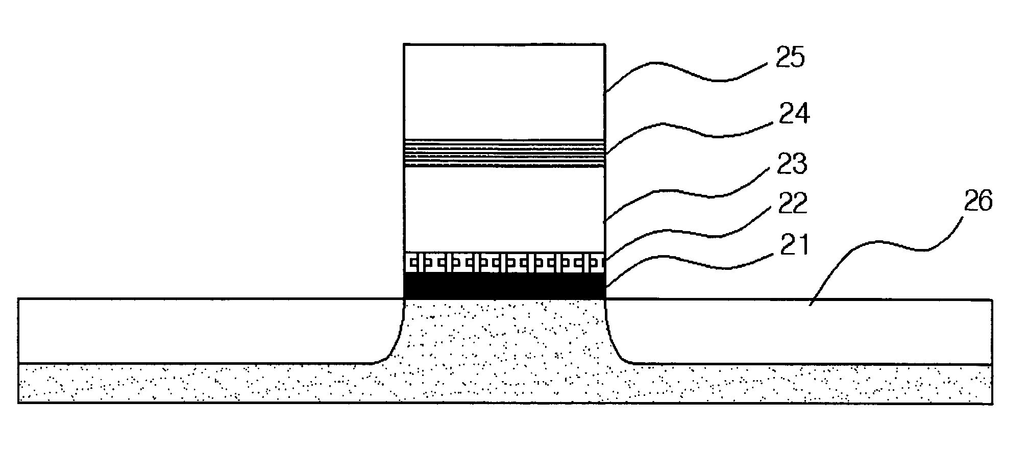
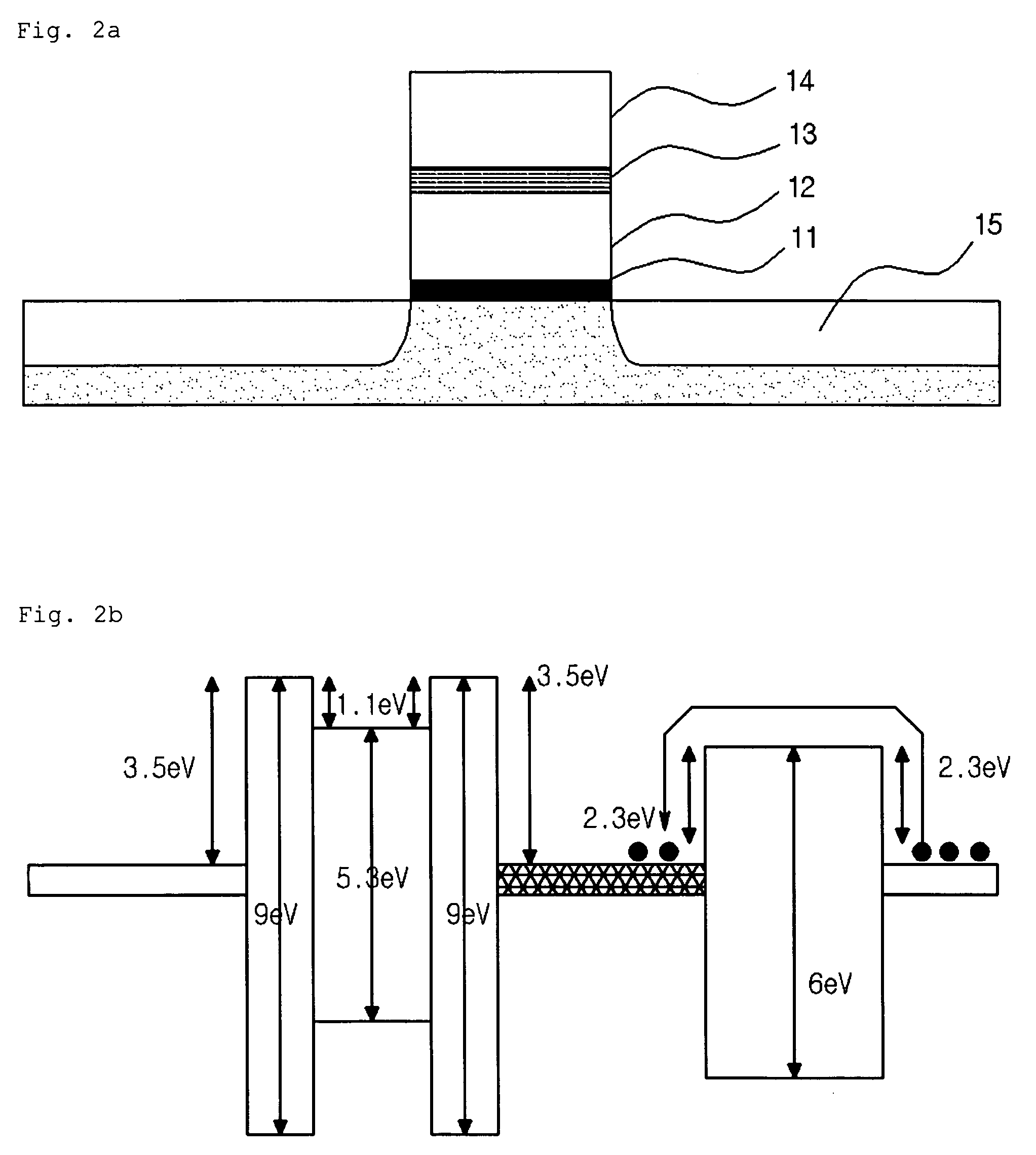
[0014]To achieve the object, the present invention provides a method for fabricating a flash memory device, the method comprising the steps of:[0015]forming a tunnel oxide layer by depositing a material with a conduction band energy level lower than that of SiO2 on a semiconductor substrate;[0016]forming a floating gate by depositing polysilicon on the tunnel oxide layer;[0017]forming an intergate dielectric layer on the floating gate;[0018]forming a control gate on the intergate dielectric layer;[0019]forming a gate electrode by patterning the tunnel oxide layer, the f...


PUM


Abstract

A method for fabricating a flash memory includes forming a tunnel oxide layer by depositing a material with a conduction band energy level lower than that of SiO2 on a semiconductor substrate; forming a floating gate by depositing polysilicon on the tunnel oxide layer; forming an intergate dielectric layer on the floating gate; forming a control gate on the intergate dielectric layer; forming a gate electrode by patterning the tunnel oxide layer, the floating gate, the intergate dielectric layer and the control gate; and forming a source / drain region by implanting impurities into the substrate using the gate electrode as a mask.

Description

BACKGROUND OF THE INVENTION[0001]1. Field of the Invention[0002]The present invention relates to a method for fabricating a flash memory device and, more particularly, to a flash memory device whose characteristics are improved by increasing efficiency of hot electron injection via changing a conduction band energy level of a tunnel oxide layer.[0003]2. Background of the Related Art[0004]FIG. 1a shows a conventional floating gate device. The conventional floating gate device can be fabricated as follows. First, SiO2 1 as a tunnel oxide layer is grown on a P-type silicon substrate. Then, a polysilicon floating gate 2 is deposited on the tunnel oxide layer. Next, an ONO (Oxide-Nitride-Oxide) layer 3 is deposited on the polysilicon floating gate in most cases to increase a coupling ratio. Thereafter, a gate is made by forming and patterning a control gate 4. Finally, a source / drain impurity region 5 is formed in the silicon substrate by performing an ion implantation process using the ...

Claims


Application Information

Patent Timeline
Patent Type & Authority Patents(United States)
IPC IPC(8): H01L27/115H01L21/28H01L21/336H01L29/423H01L29/51
CPCH01L21/28194H01L21/28273H01L29/42324H01L29/513H01L29/517H01L29/40114H10B69/00
Inventor JUNG, JIN HYO
Owner MARVELL ASIA PTE LTD
Why Eureka
Try Eureka