Semiconductor memory device capable of improving quality of voltage waveform given in a signal interconnection layer

a memory device and signal interconnection layer technology, applied in memory systems, solid-state devices, instruments, etc., can solve problems such as disturbance in the flow of return current, degradation, and degradation of signal quality, and achieve the effect of improving the quality of voltage waveform

Active Publication Date: 2005-12-20
LONGITUDE LICENSING LTD
View PDF12 Cites 15 Cited by
  • Summary
  • Abstract
  • Description
  • Claims
  • Application Information

AI Technical Summary

Benefits of technology

[0012]It is therefore an object of the present invention to provide a semiconductor memory device which is capable of improving a quality of a voltage waveform given in a signal interconnection layer.

Problems solved by technology

However, when the semiconductor memory device is operated at the high frequency of several hundreds of megahertz or more, various problems occurred which are no problem in a case of operating at a low frequency.
That is, it was known in the semiconductor memory device comprising the above-mentioned memory transmission system that the voltage waveform of the signal is largely disturbed when the signal having the high frequency is outputted on the signal interconnection and degradation of a signal quality occurs.
However, in a case where opposite layers of the bus in the memory module and the mother board are different from each other, it was understood that disturbance occurs in a flow of the return current and degradation happens in a transmission signal of the bus caused by this.
When the conductive layer opposite to the signal interconnection layer changes from the ground layer to the power supply layer or from the power supply layer to the ground layer in the manner which is described above, it was understood that a phenomenon so that disturbances occur in a waveform of the return current flowing in the conductive layer caused by an impedance mismatching or the like is found and the disturbances of the waveform of the return current have a bad influence for quality of a voltage waveform of the signal in the signal interconnection layer.

Method used


Image

  • Semiconductor memory device capable of improving quality of voltage waveform given in a signal interconnection layer
  • Semiconductor memory device capable of improving quality of voltage waveform given in a signal interconnection layer
  • Semiconductor memory device capable of improving quality of voltage waveform given in a signal interconnection layer

Examples


Embodiment Construction

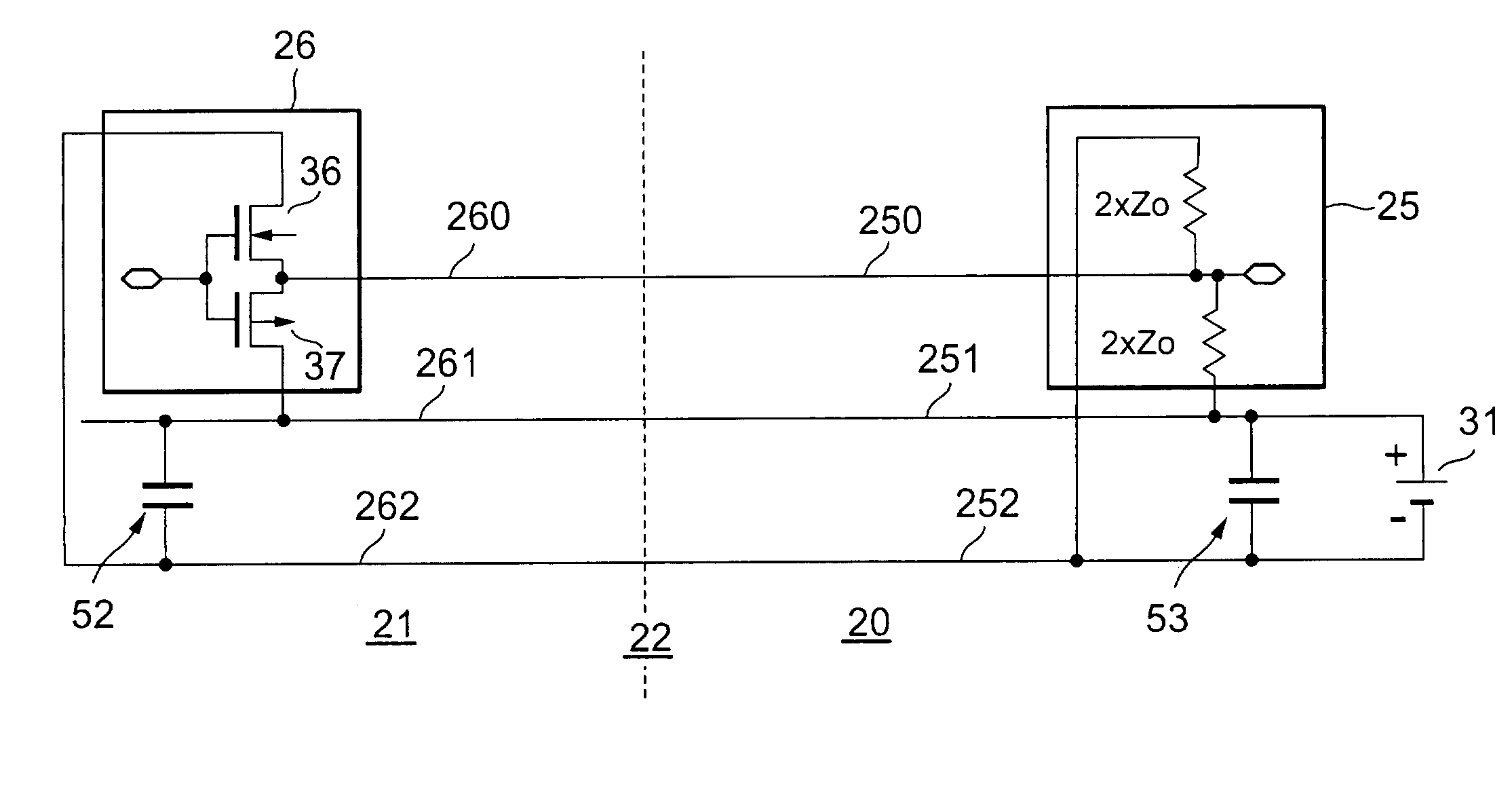
[0045]Referring to FIG. 1, a conventional semiconductor memory device will be described at first in order to facilitate an understanding of the present invention. FIG. 1 is a view for use in describing a bus transmission structure in the conventional memory device.

[0046]The illustrated semiconductor memory device comprises a mother board 20 and a memory module 21 mounted on the mother board 20. On each of the mother board 20 and the memory module 21, board and module multilayer interconnection are subjected. The board multilayer interconnections of the mother board 20 and the module multilayer interconnections of the memory module 21 are electrically connected to each other through a connector 22. On the mother board 20, a memory controller 25 is mounted. On the memory module 21, a memory device is mounted. In the example being illustrated, although illustration is made in a case where a single memory device 26 is mounted on the memory module 21 in order to simplify the description,...


PUM


Abstract

In a multilayer interconnection layer of a mother board and a memory module, a position relationship between a bus interconnection layer and a conductive layer of a power supply layer or a ground layer opposite to the bus interconnection layer is substantially held in not only the mother board but also the memory module and a relationship of multilayer interconnections is unified. As a result, it is possible to reduce disturbance of a return current of a high frequency signal given to the bus interconnection layer, to prevent degradation of quality of a signal waveform caused by the disturbance of the return current, and to prevent unnecessary electromagnetic waves from radiating caused by the disturbance of the return current. When a position relationship between the bus interconnection layer and an opposite conductive layer is not held at a constant, a similar effect is obtained by disposing a bypass capacitor in the vicinity of a portion where a plane of the bus interconnection layer and the conductive layer is switched.

Description

BACKGROUND OF THE INVENTION[0001]This invention relates to a memory bus transmission system for use in a semiconductor memory device or the like and, in particular, to a semiconductor memory device comprising a memory controller and a memory device mounted on a mother board and a memory bus transmission system therefor.[0002]In general, the semiconductor memory device of the type described comprises a mother board and a memory module mounted on the mother board through a connector. In this event, a memory controller is mounted on the mother board and a plurality of memories are mounted on the memory module. The memory controller and the memory module are electrically connected to each other through signal interconnections given with high frequency signals such as a reference clock interconnections, data connections, and so on and are also electrically connected to each other through a ground interconnection and a power supply interconnection. In the semiconductor memory device of th...

Claims


Application Information

Patent Timeline
Patent Type & Authority Patents(United States)
IPC IPC(8): G11C11/41G06F12/00G11C5/00G11C5/06G11C5/14G11C11/401H01L21/82H01L21/822H01L27/04
CPCG11C5/063G11C5/14
Inventor ISA, SATOSHINISHIO, YOJI
Owner LONGITUDE LICENSING LTD
Why Eureka
Try Eureka