Substrate processing apparatus and substrate transferring method

a substrate and processing apparatus technology, applied in the direction of photosensitive materials, instruments, furnaces, etc., can solve the problems of damage to the wafer transfer device or the transfer-in stage, damage to the transfer-out stage, and the control of the wafer transfer device not being able to gain access to the transfer-out stage, so as to prevent the operation of the substrate transfer device

Active Publication Date: 2006-01-03
TOKYO ELECTRON LTD
View PDF6 Cites 9 Cited by
  • Summary
  • Abstract
  • Description
  • Claims
  • Application Information

AI Technical Summary

Benefits of technology

[0013]A first object of the present invention is to provide a substrate processing apparatus and a substrate transferring method, which make it possible to prevent the operation of the substrate transfer device from being stopped in the case where the receiving side of the substrate abruptly inhibits the transfer of the substrate when the substrate transfer device transfers the substrate.

Problems solved by technology

On the other hand, where a transfer-out signal is not transmitted from the light exposure device, the wafer transfer device is controlled not to be capable of gaining access to the transfer-out stage.
On the other hand, where the inhibiting signal is neglected so as to cause the wafer to be transferred onto the transfer-in stage, it is possible for the delivery of the wafer onto the transfer-in stage to result in failure so as to generate problems.
Also, damages are done to the wafer transfer device or the transfer-in stage.
On the other hand, where the inhibiting signal is neglected so as to cause the wafer transfer device to be urged to gain access to the transfer-out stage, it is possible for the delivery of the wafer to result in failure so as to give rise to problems.
Also, damages are done to the wafer transfer device and the transfer-out stage.

Method used


Image

  • Substrate processing apparatus and substrate transferring method
  • Substrate processing apparatus and substrate transferring method
  • Substrate processing apparatus and substrate transferring method

Examples


Embodiment Construction

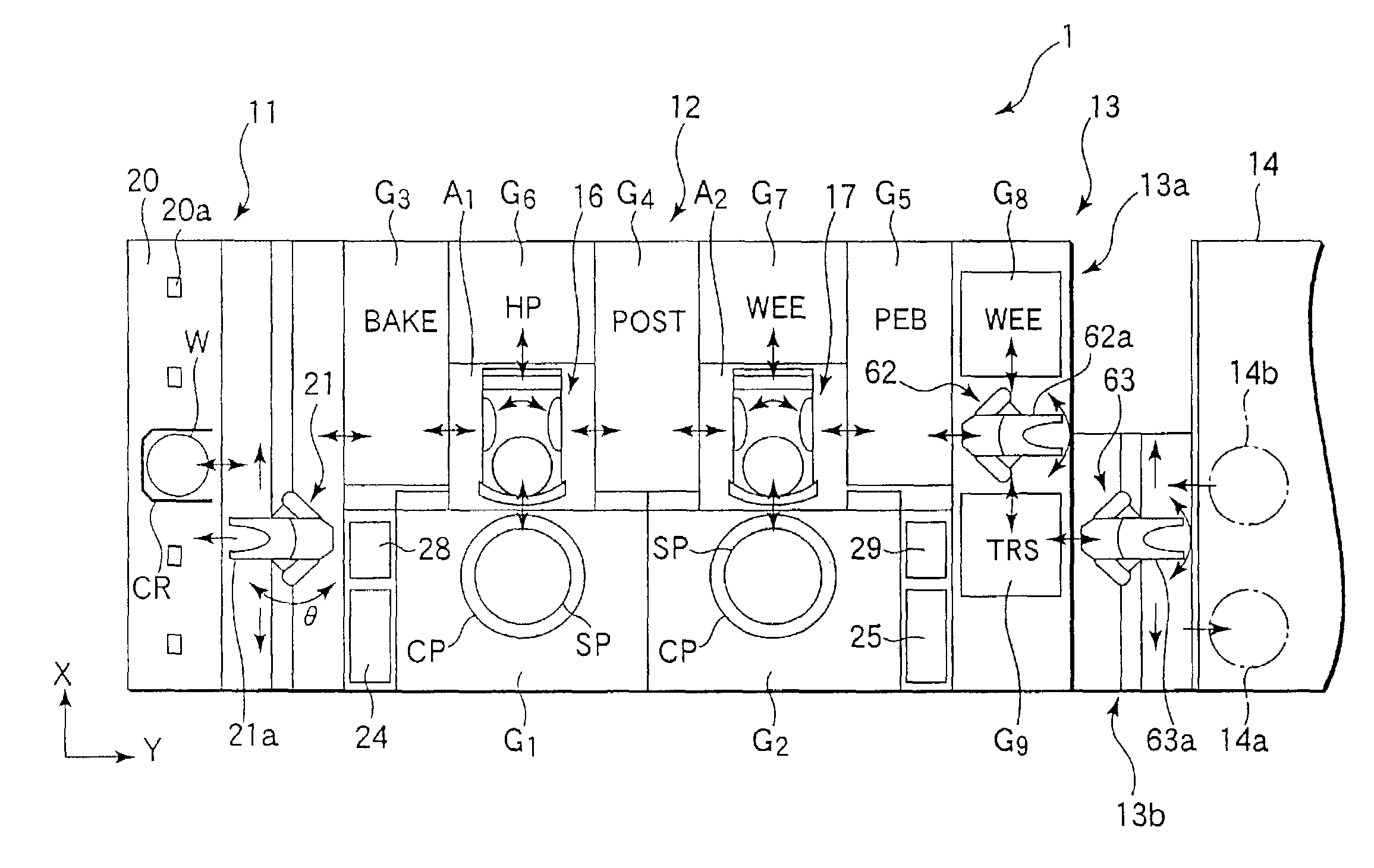
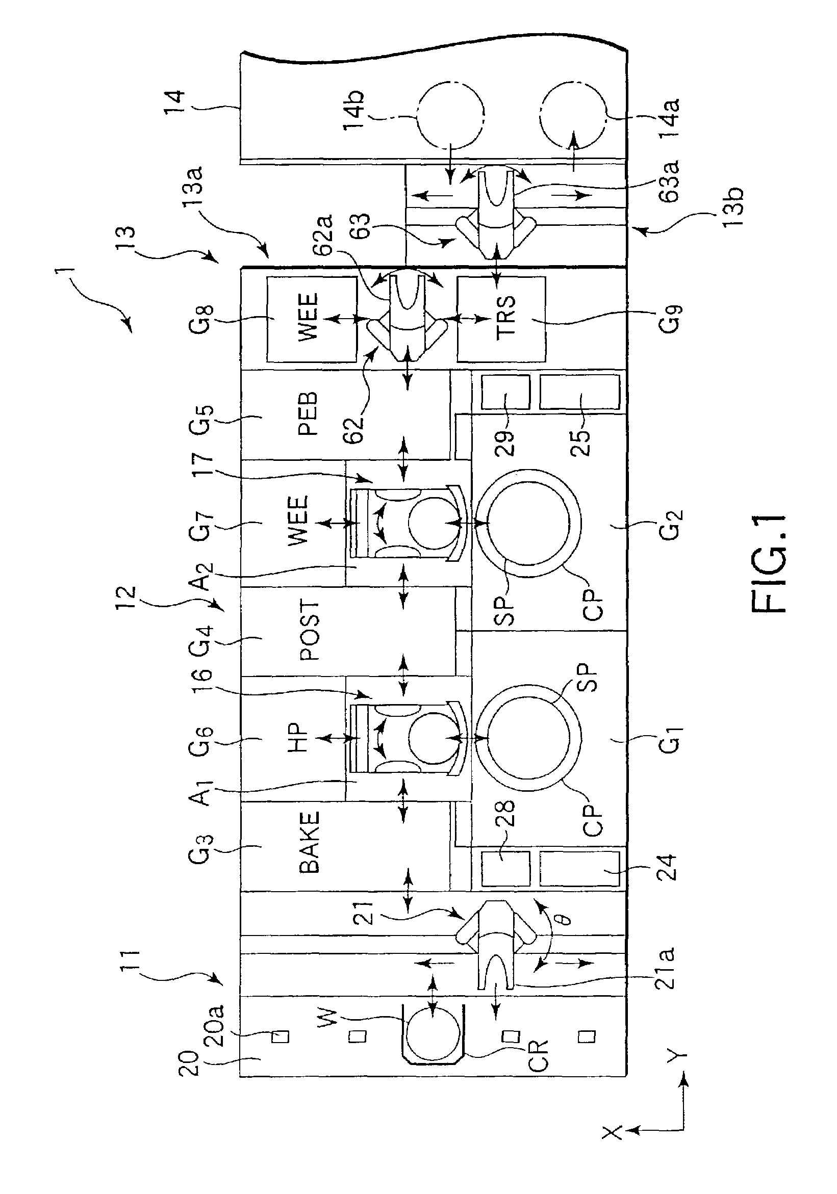
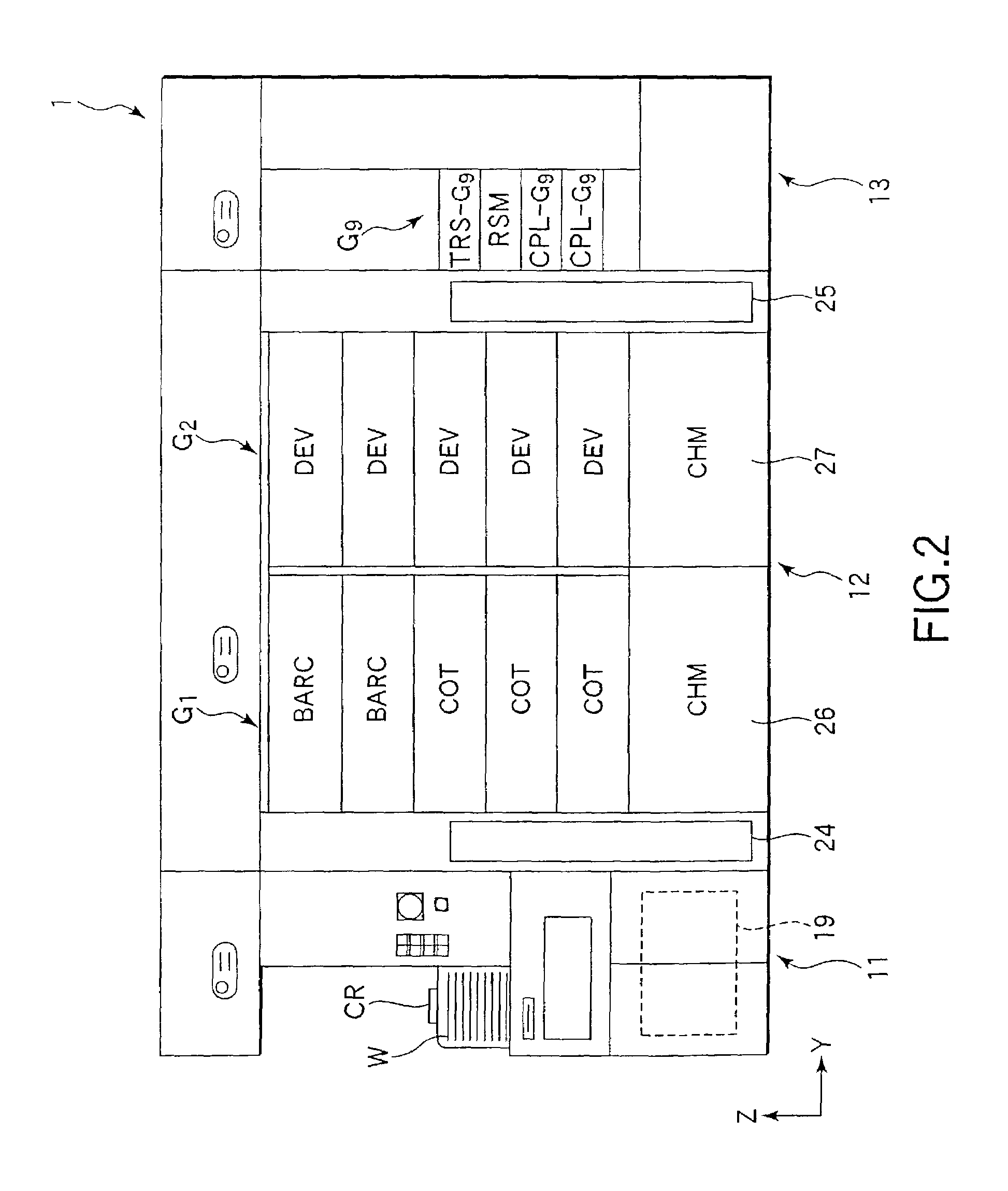
[0105]Some embodiments of the present invention will now be described in detail with reference to the accompanying drawings. The following description covers a resist coating / developing system in which a semiconductor wafer is coated with a resist solution and the wafer exposed to light is subjected to a developing processing. FIG. 1 is a plan view schematically showing the construction of a resist coating / developing system 1, and FIGS. 2 and 3 are a front view and a back view, respectively, schematically showing the construction of the resist coating / developing system 1 shown in FIG. 1.

[0106]As shown in the drawings, the resist coating / developing system 1 comprises a cassette station 11 acting as a transfer station, a process station 12 including a plurality of process units, and an interface station 13 for transferring a wafer W between a light exposure device 14 arranged adjacent to the process station 12 and the process station 12.

[0107]A wafer cassette CR housing a plurality of...


PUM

PropertyMeasurementUnit
timeaaaaaaaaaa
waiting timeaaaaaaaaaa
timeaaaaaaaaaa

Abstract

A resist coating/developing system comprises a cassette station, a process station, and an interface station. A second wafer transfer member for transferring the wafer from a high precision temperature control unit mounted to the interface station to an in-stage of a light exposure device provisionally disposes the wafer held by the second wafer transfer member on a restoration unit in the case where the wafer was taken out from the high precision temperature control unit because it was possible to transfer the wafer onto the in-stage, but it was rendered impossible later to transfer the wafer W onto the in-stage.

Description

BACKGROUND OF THE INVENTION[0001]1. Field of the Invention[0002]The present invention relates to a substrate processing apparatus for coating, for example, a semiconductor wafer with a resist solution, followed by developing the resist film after the light exposure, and a substrate transferring method in a substrate processing apparatus.[0003]2. Description of the Related Art[0004]In the manufacture of, for example, a semiconductor device, employed is a photolithography technology in which a semiconductor wafer is coated with a resist solution so as to form a resist film, followed by exposing the resist film to light by using a photo mask and subsequently developing the resist film after the light exposure so as to form a desired resist pattern on the substrate. It was customary in the past to use a resist coating / developing system for carrying out the series of processes described above.[0005]The particular resist coating / developing system is equipped with various process units for...

Claims


Application Information

Patent Timeline
Patent Type & Authority Patents(United States)
IPC IPC(8): G03D5/00B65G49/07B65H1/00H01L21/677G03D3/00G03F7/20H01L21/027
CPCG03D3/00G03F7/7075Y10S414/135H01L21/027
Inventor MIYATA, AKIRAHIGASHI, MAKIOWADA, SHIGEKI
Owner TOKYO ELECTRON LTD
Why Eureka
Try Eureka