
Eureka
For R&D, Eureka makes reading and utilizing patents & technical documents easy.
Eureka AIR
Designed for self-driven R&D workflows. Generate viable solutions, solve complex R&D challenges, empower your innovation with AI.

Eureka Materials
Designed for material experts only. Revolutionize your material R&D, from search, analyze, to developing new materials.

TechResearch
Generate reliable direction feasibility study reports for your R&D in just a few steps.

TechSeek
Discover and master advanced knowledge NOW. Basics, ideas, possibilities, all at once.

TechMind
As an expert in R&D Theories, TechMind can generates customized viable solutions instantly.

TechRisk
Analyze your overall solution with one click, know your potential R&D risks in advance.

TechMonitor
Get weekly tech updates, stay abreast of the latest tech innovations and key insights.
Method and system for manufacturing a pixel image sensor
- Summary
- Abstract
- Description
- Claims
- Application Information
AI Technical Summary
Benefits of technology
Problems solved by technology
Method used
Image

Examples
Embodiment Construction
[0030]The following description and drawings are illustrative of the invention and are not to be construed as limiting the invention. Numerous specific details are described to provide a thorough understanding of the present invention. However, in certain instances, well known or conventional details are not described in order to avoid obscuring the description of the present invention.
[0031]In at least one embodiment of the present invention, a lateral photodiode element is closely coupled to a vertical overflow drain system to provide a pixel image sensor that has a large fill factor and a large dynamic range.
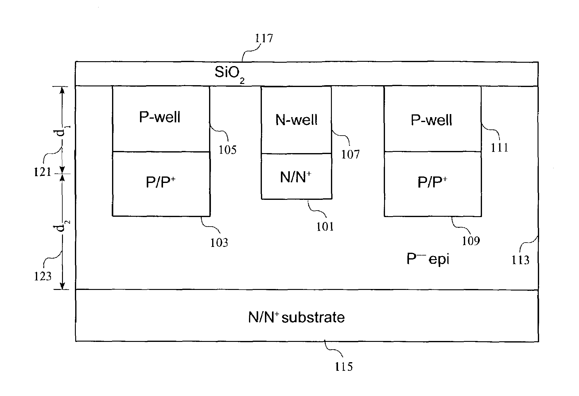
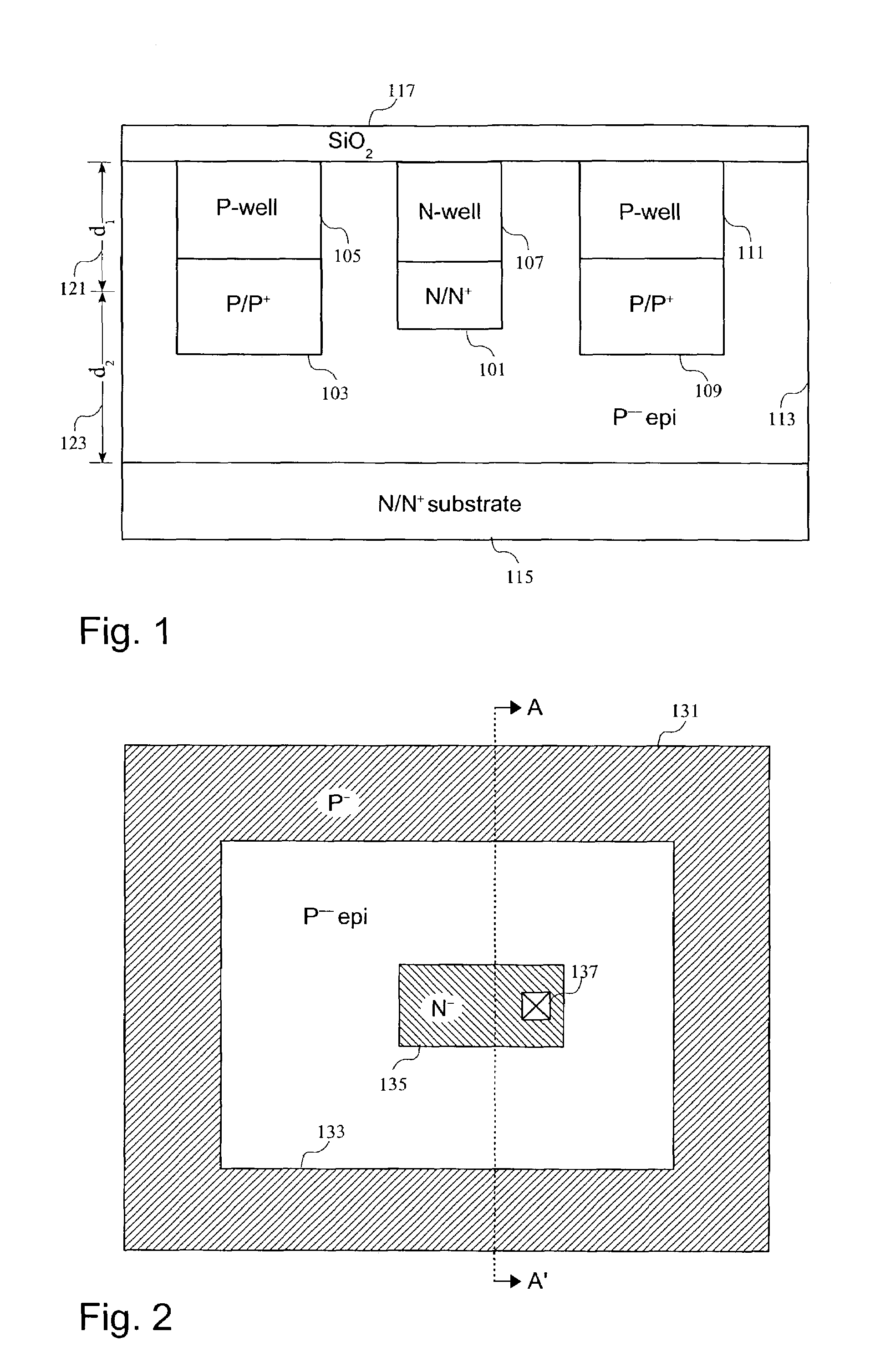
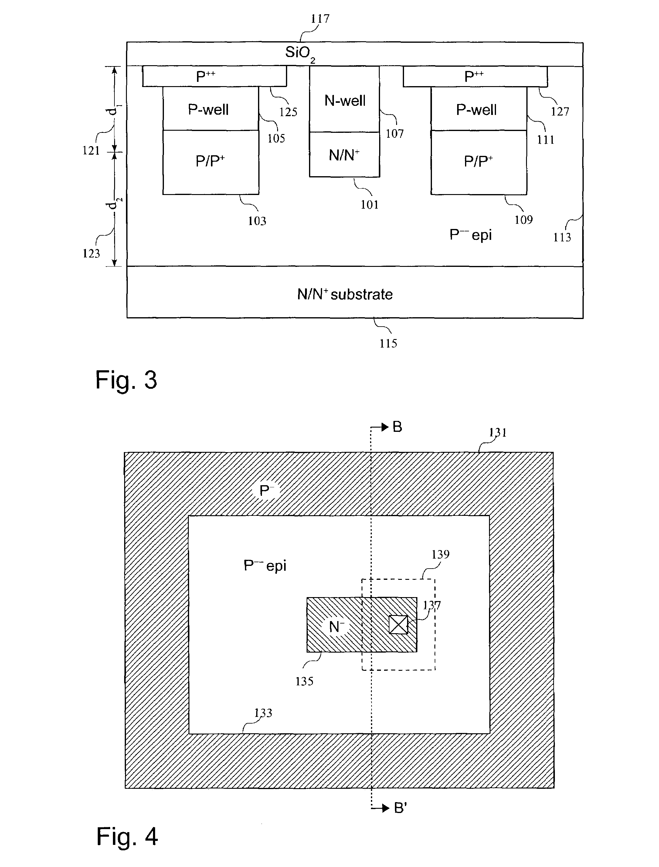
[0032]FIG. 1 shows a cross section view of a pixel image sensor according to one embodiment of the present invention. In FIG. 1, the pixel image sensor is formed on top of N-type substrate 115 (e.g., doped with Phosphorous to a density of 1E15 atoms / cm3 to 1E18 atoms / cm3). N-type regions 101 and 107 are surrounded by P-epi semiconductive material (e.g., doped with Boron to a ...
PUM
 Abstract
Description
Claims
Application Information
 - R&D Engineer
- R&D Manager
- IP Professional
- Industry Leading Data Capabilities
- Powerful AI technology
- Patent DNA Extraction
Browse by: Latest US Patents, China's latest patents, Technical Efficacy Thesaurus, Application Domain, Technology Topic, Popular Technical Reports.
© 2024 PatSnap. All rights reserved.Legal|Privacy policy|Modern Slavery Act Transparency Statement|Sitemap|About US| Contact US: help@patsnap.com