Surface acoustic wave device and method for producing the same

Inactive Publication Date: 2006-01-10
PANASONIC CORP
View PDF15 Cites 1 Cited by
  • Summary
  • Abstract
  • Description
  • Claims
  • Application Information

AI Technical Summary

Benefits of technology

[0012]In the above-described surface acoustic wave device, the depth of the doping region may be not more than 50 nm. Most of the surface acoustic waves that propagate on the surface of the SAW device propagate in a region in a depth up to about ¼ of the wavelength of the surface acoustic wave from the surface of the substrate. In the case of a SAW device with a 2 GHz band using LiNbO3, the surface acoustic waves propagate in a region in a depth up to about 0.5 μm from the surface of the substrate. This embodiment can provide a SAW device having particularly good characteristics for propagation of the surface acoustic waves, because the doping region is sufficiently thin relative to the region for propagation.
[0032]As described above, the SAW device of the present invention and the method for producing a SAW device of the present invention easily provide a surface acoustic wave device in which discharge between the IDT electrodes hardly occurs and that has good characteristics for SAW propagation. The present invention is useful for various SAW devices such as ladder type or traveling-wave type SAW filters or SAW resonators.

Problems solved by technology

The discharge between the electrodes causes melting and cutting-off of the electrodes, resulting in deterioration or shift of the characteristics of the filter.
However, since this metal electrode is fine, the electric connection is easily broken, for example by heat.
Thus, this method cannot provide a reliable filter.
However, in the above method, since the IDT electrodes are covered with the thin film, the characteristics for propagation of surface acoustic waves may be deteriorated.
However, the SAW filter obtained by the third method has a problem in that insertion loss of high frequency characteristics is increased.
It is believed that this is caused by lattice defects generated significantly deep in the substrate when the substrate is treated with heat in a reducing gas, which affects the propagation of the surface acoustic wave energy.

Method used


Image

  • Surface acoustic wave device and method for producing the same
  • Surface acoustic wave device and method for producing the same
  • Surface acoustic wave device and method for producing the same

Examples


embodiment 1

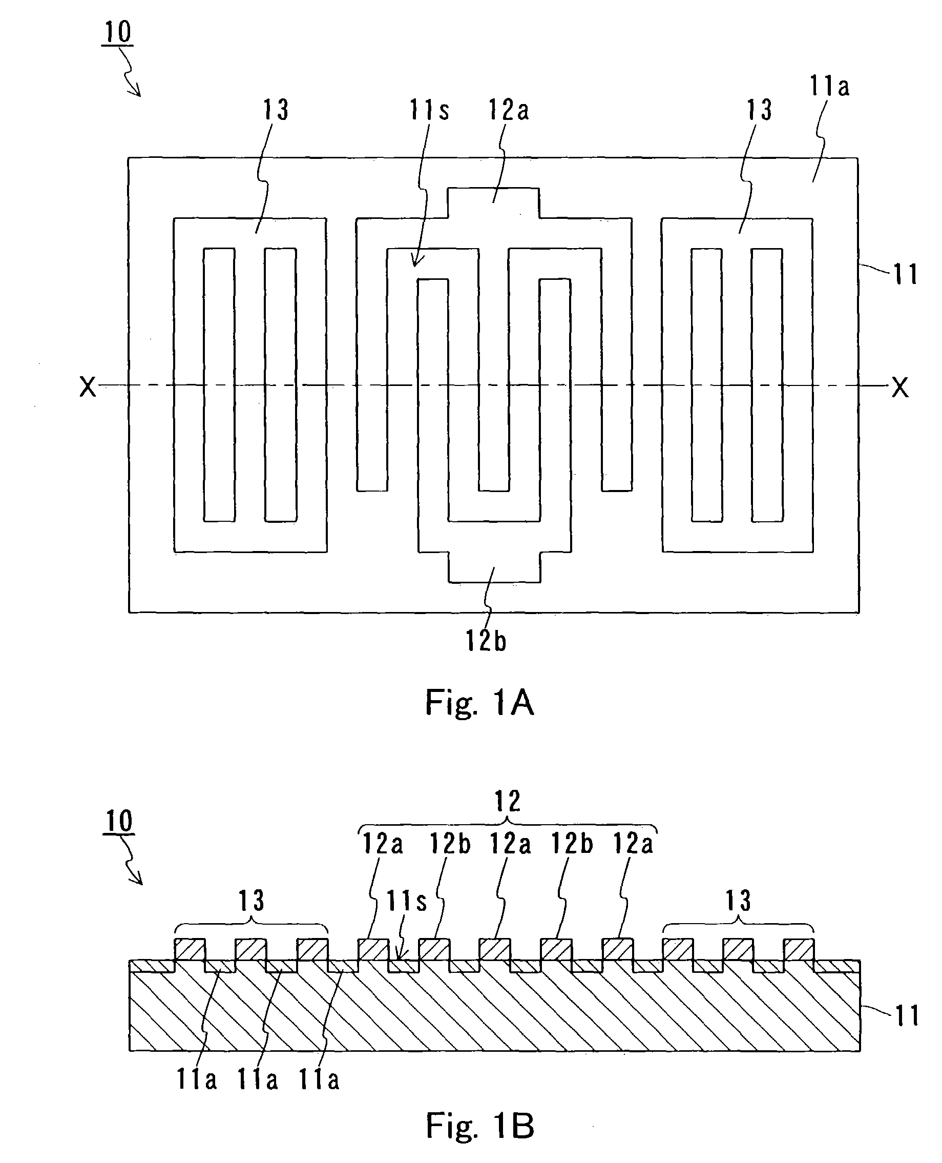
[0049]In Embodiment 1, a SAW device of the present invention will be described. FIG. 1A is a plan view of a SAW device 10 of Embodiment 1. FIG. 1B is a cross-sectional view of the SAW device 10 taken along line X—X.

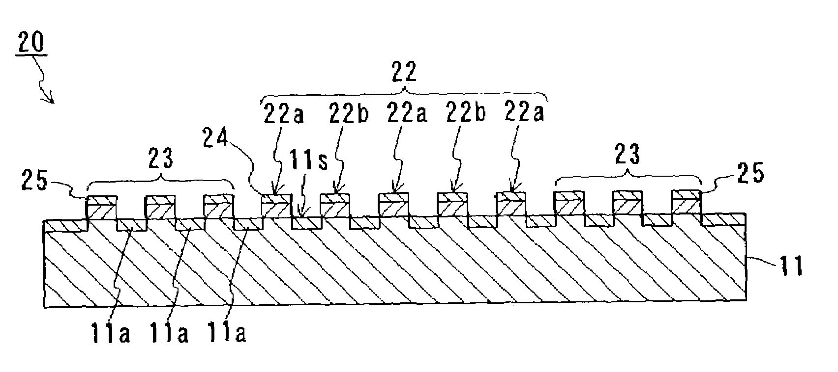
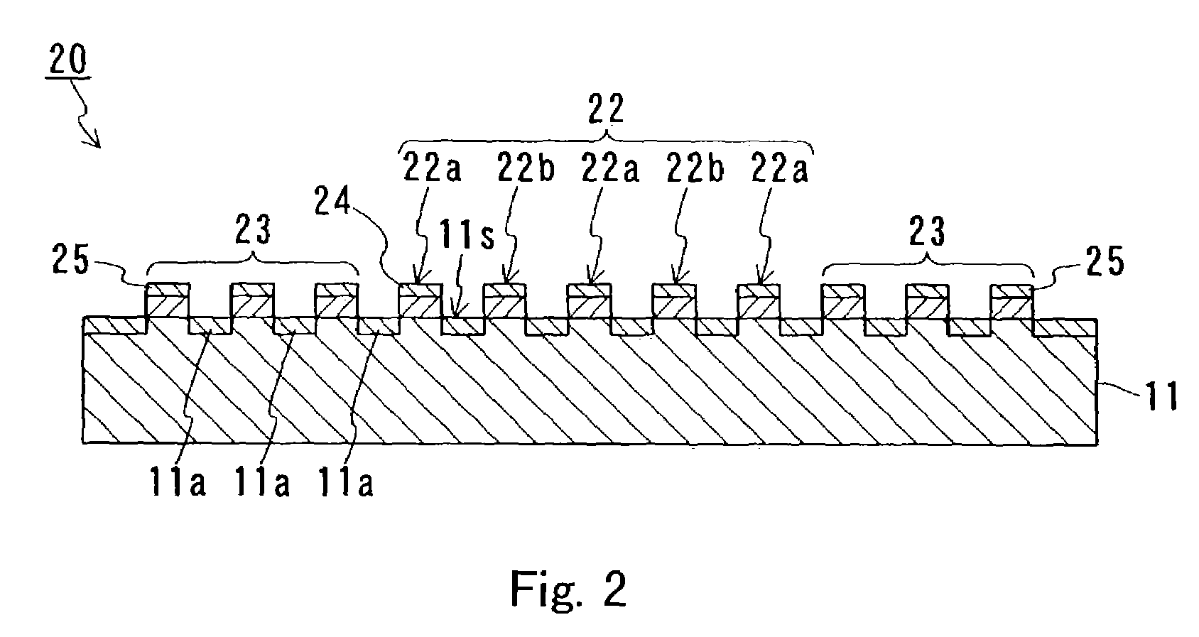
[0050]Referring to FIGS. 1A and 1B, the SAW device 10 includes a substrate 11, a pair of IDT electrodes 12 formed on the substrate 11, and reflectors 13 formed on the substrate 11. The pair of IDT electrodes 12 includes a first IDT electrode 12a and a second IDT electrode 12b. The substrate 11 includes a doping region 11a in a substrate surface 11s between the first IDT electrode 12a and the second IDT electrode 12b and between the IDT electrodes 12 and the reflectors 13. The SAW device 10 includes electric wires or pad electrodes, if necessary. Furthermore, the SAW device of the present invention may include a plurality of sets of IDT electrodes on the substrate.

[0051]A substrate having a piezoelectric property and a pyroelectric property can be used as the substrate 11....

embodiment 2

[0069]In Embodiment 2, a method of the present invention for producing a SAW device will be described. The same components as those described in Embodiment 1 bear the same reference numerals, and duplicate description will be omitted.

[0070]The method of Embodiment 2 includes (a) forming a first IDT electrode and a second IDT electrode on a piezoelectric substrate in such a manner that the first IDT electrode and the second IDT electrode are opposed to each other. Hereinafter, this process may be referred to as process (a).

[0071]Furthermore, this method includes (b) forming a doping region in a surface of the substrate by doping the surface of the substrate between the first IDT electrode and the second IDT electrode with a substance in at least one form selected from the group consisting of atoms, molecules and clusters before or after the process (a). Hereinafter, this process may be referred to as process (b). The substance with which the substrate is doped may be in the form of i...

example 1

[0090]In Example 1, an example of a method for producing a SAW device of the present invention will be described. FIGS. 6A to 6D show a production process sequence of Example 1.

[0091]First, as shown in FIG. 6A, a substrate 61 made of LiTaO3 is prepared, and the surface thereof is washed. Then, as shown in FIG. 6B, a doping region 61a having a sheet resistance in the range from 108Ω / □ to 1015Ω / □ is formed in the substrate 61. The doping region 61a can be formed by doping the substrate 61 with boron ions by plasma doping. The doping of boron ions can be performed under the conditions of an implantation energy of 700 eV and a dose of 1×10¹⁶ ions / cm2.

[0092]Then, as shown in FIG. 6C, a metal film 62 (a thickness of 800 nm) made of aluminum is formed over the substrate 61 by sputtering.

[0093]Then, as shown in FIG. 6D, IDT electrodes 63a and 63b are formed by removing unnecessary portions in the metal film 62. The IDT electrodes are formed in the following manner. First, a resist film (a t...


PUM


Abstract

A surface acoustic wave device includes a piezoelectric substrate, a first interdigital transducer and a second interdigital transducer formed on the substrate so that the first and second interdigital transducers are opposed to each other. The substrate includes a doping region that is doped with a substance in at least one form selected from the group consisting of atoms, molecules and clusters in a surface between the first and second interdigital transducers.

Description

BACKGROUND OF THE INVENTION[0001]1. Field of the Invention[0002]The present invention relates to a surface acoustic wave device and a method for producing the same.[0003]2. Description of the Related Art[0004]A surface acoustic wave device is used, for example, in a high frequency circuit of cellular phones. FIG. 12 shows a SAW filter 1 in a plan view as an example of a conventional surface acoustic wave device (hereinafter, referred to also as a SAW device). The SAW filter 1 includes a piezoelectric substrate 2 and a pair of interdigital transducers 3a and 3b (hereinafter, referred to also as IDT electrodes) formed on the substrate 2. The substrate 2 is formed of LiTaO3, LiNbO3 or the like.[0005]In the SAW filter 1, if the substrate 2 has a pyroelectric property, a change in temperature in an assembly process or a change in temperature when used as a device causes non-uniformity in electric charge distribution on the surface of the substrate 2. As a result, a potential difference i...

Claims


Application Information

Patent Timeline
IPC IPC(8): H01L21/00H03H9/02
CPCH03H9/02645H03H9/02921H03H9/14541H03H3/08H01L2224/48227H01L2924/01046H01L2924/01078H01L2924/01019
Inventor TAKASE, MITIHIKOOKAJIMA, MICHIOYOSHIDA, AKIHISASETSUNE, KENTAROMURAKAMI, KOUZOUFUJII, KUNIHIRO
Owner PANASONIC CORP
Why Eureka
Try Eureka