

Laser module and optical head
a laser module and optical head technology, applied in the field of laser modules, optical heads or optical information recording and reproduction apparatuses, can solve the problems of reducing the need for optical heads whose optical efficiency is difficult to be changed, etc., and achieves the reduction of the optical efficiency of the optical head system and the reduction of the optical efficiency of each laser beam.
- Summary
- Abstract
- Description
- Claims
- Application Information
AI Technical Summary
Benefits of technology
Problems solved by technology
Method used
Image

Examples
first embodiment
[0039]In the following, the present invention will be described by using FIG. 1 to FIG. 5.
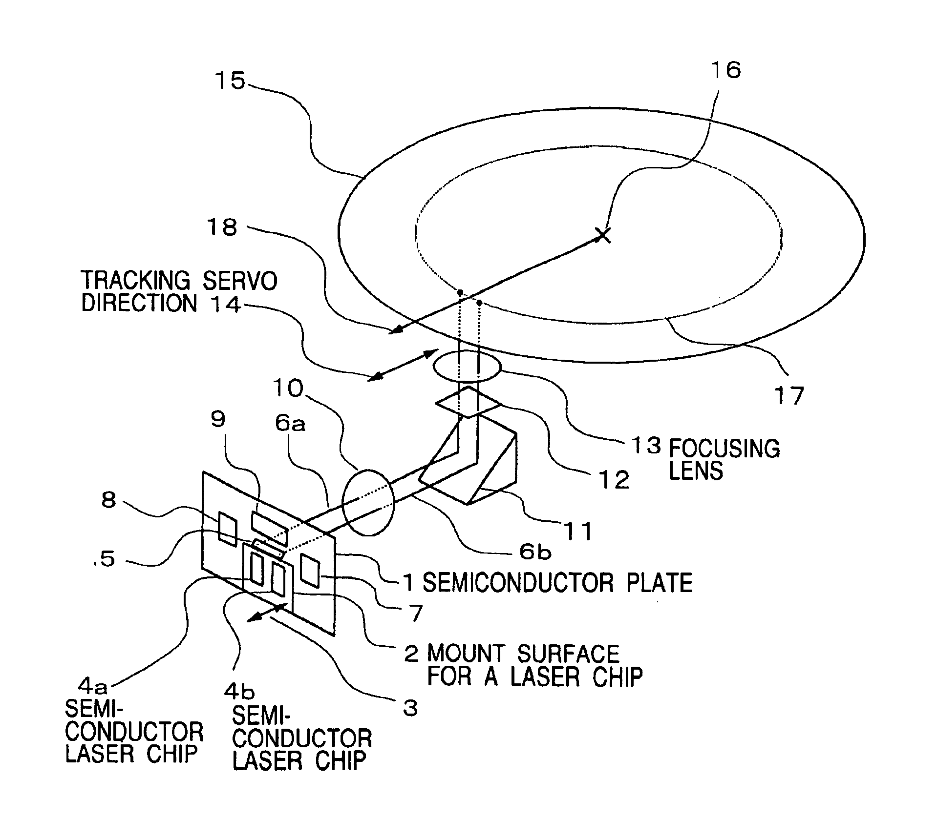
[0040]FIG. 1 shows the basic constitution of the optical disk unit and the optical head using the present invention. Reference numeral 1 denotes the semiconductor plate where the photodetecting elements, the electronic circuit and the like are formed on its surface, the laser chips and the like are mounted thereon, and silicon or the like is preferable, for example. In FIG. 1, the front surface of the semiconductor plate 1 cannot be seen actually because it is arranged facing its rear surface to a viewer, but the drawing shows in a phantom state where the plate is seen from the rear surface to the front surface. 2 denotes the mount surface for the laser chips, which is formed by engraving the surface of the semiconductor plate 1 in the depth of approximately 30 μm to 100 μm by etching processing or the like, and the mount surface for the laser chips 2 is parallel with the surface of the semicon...
second embodiment
[0051]FIGS. 11(a) and 11(b) show the structure of the optical disk unit using the present invention, in which 11(a) is a plan view and 11(b) is a side view. 111 denotes the case of the optical disk unit. 112 denotes the motor mounted on the case 111 of the optical disk unit to rotate the optical disk 15 via the shaft 103. 114 denotes the optical head where the package 81 enclosing the semiconductor plate 61 and the lens actuator 115 mounted with the focusing lens 13 are mounted. 106 denotes the access mechanism mounted on the optical head 114, and 107 denotes the rail mounted on the case 111 of the optical disk unit. The optical head 114 can move on the rail 107 by the access mechanism 116 in the radius direction of the disk 15. The collimating lens 10, the mirror 71 and the composite element 12 are inside of the optical head 114. The laser beam 66a or 66b radiated from the semiconductor laser chip 4a or 4b mounted on the package 81 is radiated from the optical head 114 via the focu...
PUM
 Abstract
Description
Claims
Application Information