Optical sensor device and electronic device including the same

a sensor device and optical sensor technology, applied in the field of optical sensors, can solve the problems of deterioration of aesthetic appeal of electronic devices, increase of production steps and/or unit costs, etc., and achieve the effects of reducing optical efficiency, minimizing energy loss, and low thickness

Inactive Publication Date: 2020-06-11
SAMSUNG ELECTRONICS CO LTD
View PDF0 Cites 0 Cited by
  • Summary
  • Abstract
  • Description
  • Claims
  • Application Information

AI Technical Summary

Benefits of technology

[0007]The light sensor device may have a relatively low thickness compared to other electronic components included in the electronic device. As an air gap increases, optical efficiency may be lowered. For this reason, in order to mount the light sensor device in the electronic device, it is desirable to utilize an interposer for minimizing energy loss caused by the air gap, which may compensate for a height difference with another electronic component. However, this may introduce a problem in production steps and / or unit costs may increase, due to the addition of the interposer for mounting the light sensor device.
[0008]In addition, due to the diversification of services, the light sensor device frequently utilizes various light-emitting elements having different wavelength bands, even as the area allocated for disposition of the light sensor device increases. As the area of the light sensor device increases, the light sensor device is increasingly exposed to the external environment of the electronic device, and thus the aesthetic appeal of the electronic device deteriorates. Accordingly, in the electronic device, there is a need for improving the design of the electronic device while maintaining and / or improving optical efficiency, and compensating for the air gap without the drawbacks of the interposer structure.
[0009]An electronic device according to certain embodiments may include: a substrate, an optical sensor device including at least one light-emitting element and a light-receiving element, the optical sensor device mounted on the substrate, and an injection-molded lens coupled to the substrate and covering the optical sensor device, wherein the injection-molded lens is spaced apart from the optical sensor device by a set distance, wherein patterns are integrally formed in at least a portion of the injection-molded lens, the patterns affecting transmission of light of at least one wavelength band to improve an optical efficiency of the transmitted light.
[0010]An electronic device according to certain embodiments may include: a circuit board including a substrate, an optical sensor device including at least one light-emitting element and a light-receiving element, the optical sensor device mounted on the substrate, and an injection-molded lens coupled to the substrate and covering the optical sensor device, wherein the injection-molded lens is spaced apart from the optical sensor device by a set distance, wherein the injection-molded lens includes a top part disposed above a top face of the optical sensor device, and a side part supporting the top part as a side face of the optical sensor device, and patterns are integrally formed in at least a portion of the injection-molded lens, the patterns affection transmission of light of at least one wavelength band to improve an optical efficiency of the transmitted light.
[0011]According to certain embodiments, an injection-molded lens having a pattern integrally formed therein to improve optical efficiency for at least one wavelength is mounted in an electronic device as a structure of covering an optical sensor device so as to compensate for a height difference between the light sensor device and another electronic component. Thus, the injection-molded lens is capable of satisfying a design requirement and improving visibility.

Problems solved by technology

However, this may introduce a problem in production steps and / or unit costs may increase, due to the addition of the interposer for mounting the light sensor device.
As the area of the light sensor device increases, the light sensor device is increasingly exposed to the external environment of the electronic device, and thus the aesthetic appeal of the electronic device deteriorates.

Method used


Image

  • Optical sensor device and electronic device including the same
  • Optical sensor device and electronic device including the same
  • Optical sensor device and electronic device including the same

Examples


Embodiment Construction

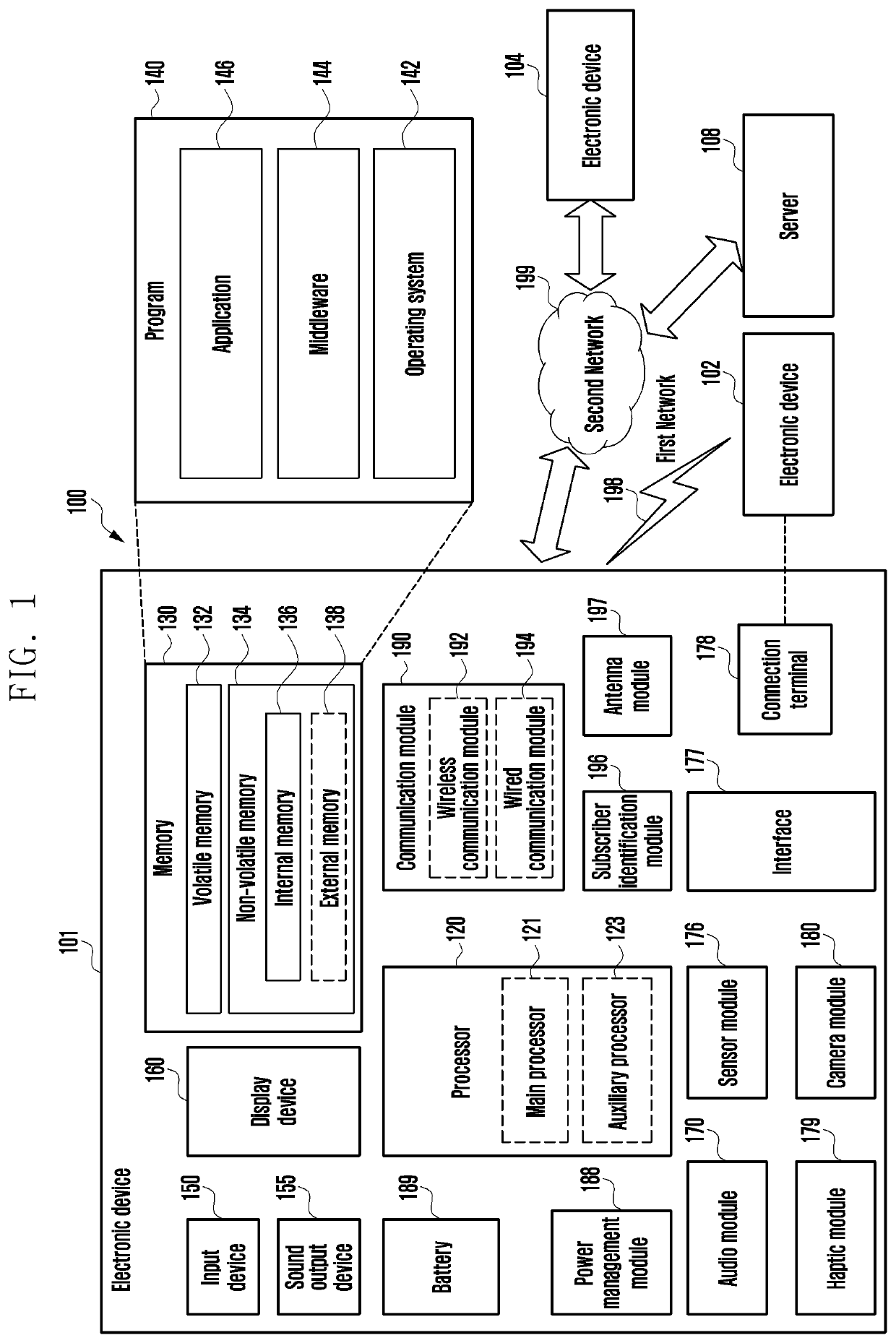
[0019]The electronic device according to certain embodiments may be one of various types of electronic devices. The electronic devices may include, for example, a portable communication device (e.g., a smart phone), a computer device, a portable multimedia device, a portable medical device, a camera, a wearable device, or a home appliance. According to an embodiment of the disclosure, the electronic devices are not limited to those described above.

[0020]FIG. 1 is a block diagram illustrating an electronic device 101 in a network environment 100 according to certain embodiments. Referring to FIG. 1, the electronic device 101 in the network environment 100 may communicate with an electronic device 102 via a first network 198 (e.g., a short-range wireless communication network), or an electronic device 104 or a server 108 via a second network 199 (e.g., a long-range wireless communication network). According to an embodiment, the electronic device 101 may communicate with the electroni...


PUM

PropertyMeasurementUnit
wavelength bandaaaaaaaaaa

Abstract

An electronic device is disclosed herein, including: a substrate, an optical sensor device including at least one light-emitting element and a light-receiving element, the optical sensor device mounted on the substrate, and an injection-molded lens coupled to the substrate and covering the optical sensor device, wherein the injection-molded lens is spaced apart from the optical sensor device by a set distance, wherein patterns are integrally formed in at least a portion of the injection-molded lens, the patterns affecting transmission of light of at least one wavelength band to improve an optical efficiency of the transmitted light.

Description

CROSS-REFERENCE TO RELATED APPLICATION(S)[0001]This application is based on and claims priority under 35 U.S.C. 119 to Korean Patent Application No. 10-2018-0159143, filed on December 11, 2018, in the Korean Intellectual Property Office, the disclosure of which is herein incorporated by reference in its entirety.BACKGROUND1) Technical Field[0002]The disclosure relates to an electronic device including light emitters and light detecting sensors, and, more particularly, to disposition of patterns in a cover of the electronic device to affect the optics of light transmitted and received by the emitters and sensors.2) Description of Related Art[0003]An electronic device may perform various functions in combination, among which include functions which utilize sensor devices. The sensor devices may collect information related to the electronic device, an external environment of the electronic device, or a user. The electronic device may provide various functions or services to the user ba...

Claims


Application Information

Patent Timeline
Patent Type & Authority Applications(United States)
IPC IPC(8): G01J1/04G02B3/08
CPCA61B3/14A61B5/4064A61B5/1172G01J1/0477A61B5/02433A61B5/021G02B3/08A61B5/1176A61B5/14532G01J1/0411A61B5/681A61B5/6898A61B5/1455A61B5/14552A61B5/02438A61B2562/0233G02B19/0009G02B19/0085G01J1/0233G01J1/0219G01J1/0209G01J1/0271G01J1/08G01J3/0208G01J3/0259G01J3/0262G01J3/0264G01J3/0272G01J3/0291G01J3/501G01J5/022G01J5/025G01J5/0265G01J5/045G01J5/0806G02B3/0012G02B3/0037G02B5/04G06F1/1684
Inventor JO, JEONGGYUPARK, HYEONGSOON
Owner SAMSUNG ELECTRONICS CO LTD
Why Eureka
Try Eureka