Method and structure for creating ultra low resistance damascene copper wiring

a damascene copper and wire technology, applied in the direction of basic electric elements, semiconductor/solid-state device manufacturing, electric apparatus, etc., can solve the problems of reducing the electrical insulation qualities of the dielectric, affecting the performance of the damascene copper wire, and the tendency to diffuse into adjacent dielectric layers, etc., to achieve low resistance and simple and available process techniques

Inactive Publication Date: 2006-01-17
BELL SEMICON LLC
View PDF4 Cites 66 Cited by
  • Summary
  • Abstract
  • Description
  • Claims
  • Application Information

AI Technical Summary

Benefits of technology

[0009]To achieve the foregoing, the present invention provides methods and structures for forming low resistance damascene copper wiring using simple and available process techniques. The processing steps applied in the embodiments of the present invention may be used to form a unique wiring structure that is better scaleable to met further copper wiring needs as the geometries used in integrated circuits continue to decrease.

Problems solved by technology

One drawback to the use of copper in the interconnects is its tendency to diffuse (i.e., leakage) into adjacent dielectric layers.
Copper diffuses easily into dielectric layers and diminishes the electrical insulation qualities of the dielectric.
This causes undesirable via and metal line resistance increases.
Moreover, the interface between the TaN and Cu at the bottom and top of via structures is a weak point in Electromigration (EM) defect testing.
Failures due to electromigration are a major reliability concern for the use of copper in forming interconnects.
Electromigration may result in voiding and thus open circuit failures.
When these voids coincide with the interfaces at the top and bottom of the vias with surrounding interconnect lines, for example between the vias and bottom metal interface, the via connection fails or becomes highly resistive.

Method used


Image

  • Method and structure for creating ultra low resistance damascene copper wiring
  • Method and structure for creating ultra low resistance damascene copper wiring
  • Method and structure for creating ultra low resistance damascene copper wiring

Examples


Embodiment Construction

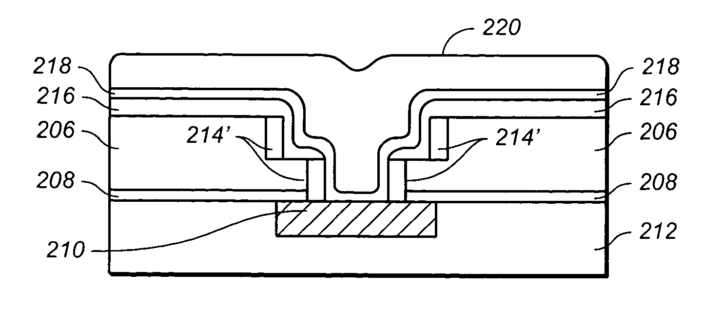
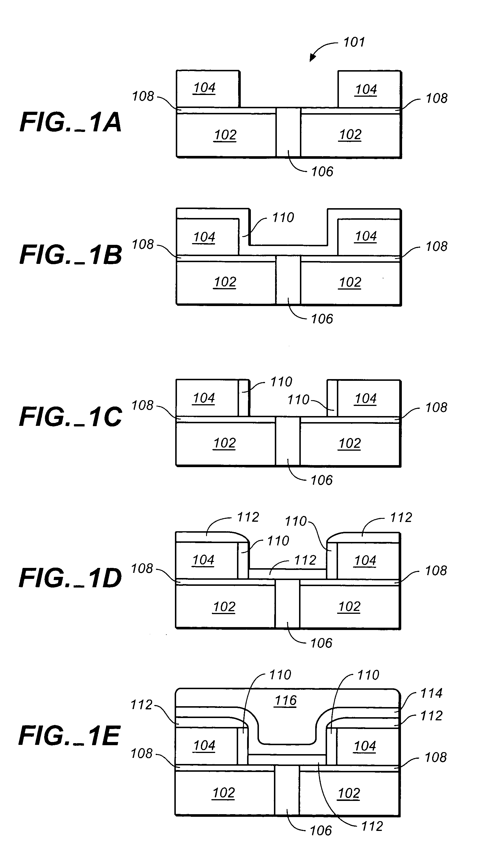
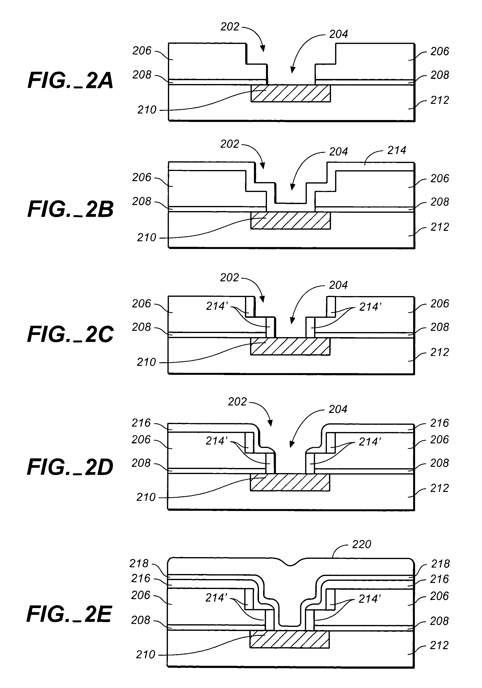
[0017]Reference will now be made in detail to preferred embodiments of the invention. Examples of the preferred embodiments are illustrated in the accompanying drawings. While the invention will be described in conjunction with these preferred embodiments, it will be understood that it is not intended to limit the invention to such preferred embodiments. On the contrary, it is intended to cover alternatives, modifications, and equivalents as may be included within the spirit and scope of the invention as defined by the appended claims. In the following description, numerous specific details are set forth in order to provide a thorough understanding of the present invention. The present invention may be practiced without some or all of these specific details. In other instances, well known process operations have not been described in detail in order not to unnecessarily obscure the present invention.

[0018]The present invention provides a thin dielectric film such as SiC or SiOC form...


PUM

PropertyMeasurementUnit
thicknessaaaaaaaaaa
thicknessaaaaaaaaaa
thicknessaaaaaaaaaa

Abstract

A low resistance copper damascene interconnect structure is formed by providing a thin dielectric film such as SiC or SiOC formed on the sidewalls of the via and trench structures to function as a copper diffusion barrier layer. The dielectric copper diffusion barrier formed on the bottom of the trench structure is removed by anisotropic etching to expose patterned metal areas. The residual dielectric thus forms a dielectric diffusion barrier film on the sidewalls of the structure, and coupled with the metal diffusion barrier subsequently formed in the trench, creates a copper diffusion barrier to protect the bulk dielectric from copper leakage.

Description

BACKGROUND OF THE INVENTION[0001]1. Field of the Invention[0002]The present invention relates to the formation of metal interconnects on semiconductor wafers. More particularly, the present invention relates to the formation of low resistance damascene copper interconnects.[0003]2. Description of the Related Art[0004]As integrated circuit devices grow smaller and smaller, higher conductance and lower capacitance is required of the interconnecting wires (i.e., interconnects). In order to accommodate these objectives, the trend has been towards the use of copper for interconnects and damascene methods for forming the interconnects. One drawback to the use of copper in the interconnects is its tendency to diffuse (i.e., leakage) into adjacent dielectric layers. Copper diffuses easily into dielectric layers and diminishes the electrical insulation qualities of the dielectric.[0005]Copper diffusion barrier layers, for example layers containing tantalum, have been deposited before the dep...

Claims


Application Information

Patent Timeline
Patent Type & Authority Patents(United States)
IPC IPC(8): H01L21/4763
CPCH01L21/76807H01L21/76843H01L21/76841H01L21/76831
Inventor BURKE, PETER A.LU, HONGQIANGSUN, SEY-SHING
Owner BELL SEMICON LLC
Why Eureka
Try Eureka