Method and apparatus for monitoring and controlling boundary scan enabled devices

a technology of boundary scan and enabled devices, which is applied in the field of integrated circuit and system testing, can solve the problems of inability to test the smaller circuits with traditional test equipment, lack of inexpensive tools, and inability to adopt boundary scan testing in general, so as to achieve simple, effective, and inexpensive manufacturing and production.

Inactive Publication Date: 2006-01-17
FOLEA JR RICHARD VICTOR
View PDF15 Cites 26 Cited by
  • Summary
  • Abstract
  • Description
  • Claims
  • Application Information

AI Technical Summary

Benefits of technology

[0019](h) to provide a simple, effective means to manually debug circuitry using boundary scan.
[0020]The present invention overcomes the above noted issues of the prior art by providing a method and apparatus that does not require the use of test vectors, test executives, netlists, or schematics to run boundary scan operations, uses a simple Light Emitting Diode (LED) and pushbutton switch graphical interface that the design community is already comfortable and familiar with, provides boundary scan cell results in real time, and is inexpensive to manufacture and produce.

Problems solved by technology

As a result, the ability to test the smaller circuits with traditional test equipment is becoming more and more of a challenge.
Unfortunately, even though the standard has been in place for over 10 years, design engineers and the electronics design community in general have not adopted boundary scan testing.
This is due to a lack of tools that are inexpensive and easy to learn and use with little or no prior understanding of boundary scan.
Without readily available easy-to-use boundary scan tools, engineers have to resort to crude trial-and-error test methodology which is expensive and time-consuming.
These costs are prohibitive for an average design engineer that simply wants to know if a part is soldered to a board correctly.
Further, while the tools that are available today are very powerful, unfortunately they are also very complicated and difficult to learn and use.
These tools have a steep learning curve and require a fundamental understanding of boundary scan that most design engineers do not have today.
This creates additional cost and complications.
Traditional boundary scan tools produce a static output report that does not lend itself to simple interactive debugging of the integrated circuits under test.

Method used


Image

  • Method and apparatus for monitoring and controlling boundary scan enabled devices
  • Method and apparatus for monitoring and controlling boundary scan enabled devices
  • Method and apparatus for monitoring and controlling boundary scan enabled devices

Examples


Embodiment Construction

—PREFERRED EMBODIMENT

[0031]Detailed descriptions of the preferred embodiments are described in the following paragraphs.
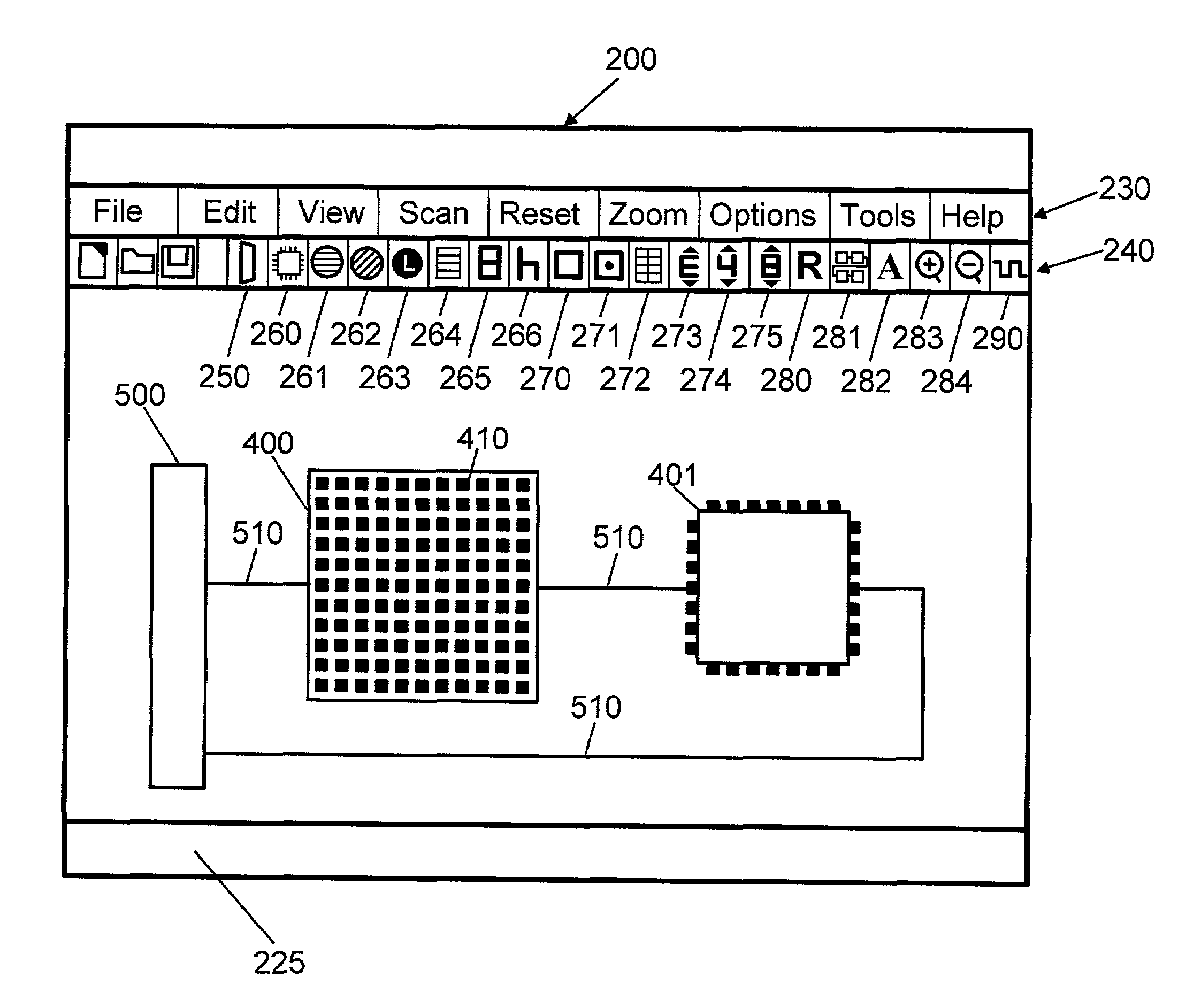
FIG. 1

[0032]FIG. 1 shows a test apparatus for carrying out the preferred embodiment of the invention. A computer 115 of the traditional type including RAM, ROM, processor, etc. is shown operatively connected by wires to a display 105, keyboard 140, mouse 110, printer 150 and interface pod 120 with interface cable 125 making the required IEEE 1149.1 boundary scan connections to the device under test (DUT) 130 through a variety of connection means. Interface pod 120 provides electrical conversion between the computer and the devices under test. Some examples are to provide electrical conversion between the Parallel port, USB port or serial port on the computer to the devices under test. The processor operates to control the program within computer 115, and receive and store data from the input devices and transmit data to the output devices. Notebook computers of sim...


PUM


Abstract

A system for monitoring and controlling boundary scan chains in real time that does not require the use of test vectors or test executives. The system automatically builds virtual Devices Under Test (DUT's) from user provided Boundary Scan Description Language (BSDL) files and displays them on the computer display. The virtual devices are connected to a port on the computer and the scan button is pressed to invoke a boundary scan. The results are displayed as color coded “pins” on a computer display to indicate if the pin is at a logic high, a logic low, or is toggling. Logic values may be forced on the pin via a point-and-click graphical user interface, again bypassing the need for test vectors. Graphical indicators and controls are provided by the system to help simplify monitoring and controlling of the boundary scan chain.

Description

CROSS-REFERENCE TO RELATED APPLICATIONS[0001]Not Applicable.FEDERALLY SPONSORED RESEARCH[0002]Not Applicable.BACKGROUND OF THE INVENTION[0003]1. Field of Invention[0004]This invention relates generally to the field of testing of integrated circuits and systems, and particularly to boundary scan testing via a machine with an interactive user interface providing real-time monitoring and control of boundary scan enabled devices and systems without requiring the use of test vectors, test executives, netlists, or schematics.[0005]2. Prior Art[0006]Each year electronic circuits and systems get smaller. As a result, the ability to test the smaller circuits with traditional test equipment is becoming more and more of a challenge. In the early 1980's, this issue was recognized and in 1985 a group of electronics and semiconductor manufacturers formed the Joint Test and Access Group (JTAG) to develop a standard for building testability features into the semiconductor devices. The standard was ...

Claims


Application Information

Patent Timeline
Patent Type & Authority Patents(United States)
IPC IPC(8): G01R31/28G01R31/00
CPCG01R31/31912G01R31/318591
Inventor FOLEA, JR., RICHARD VICTOR
Owner FOLEA JR RICHARD VICTOR
Why Eureka
Try Eureka