Conformal barrier liner in an integrated circuit interconnect

a barrier liner and integrated circuit technology, applied in the field of semiconductor technology, can solve the problems of short circuits in the integrated circuit, relatively high electrical resistance, and relatively poor adhesion of nitride compounds to copper, and achieve good barrier resistance to electro-migration, improve adhesion, and reduce size

Inactive Publication Date: 2006-01-24
INNOVATIVE FOUNDRY TECH LLC
View PDF6 Cites 31 Cited by
  • Summary
  • Abstract
  • Description
  • Claims
  • Application Information

AI Technical Summary

Benefits of technology

[0031]The present invention provides an integrated circuit having a substrate and a semiconductor device thereon. A stop layer over the substrate has a dielectric layer formed thereon having an opening into which a conformal barrier is formed. A conformal barrier liner is formed in the opening, processed, and treated to improve adhesion. Portions of the

Problems solved by technology

High barrier resistance is necessary with conductor materials such as copper to prevent diffusion of subsequently deposited copper into the dielectric layer, which can cause short circuits in the integrated circuit.
However, these nitride compounds also have relatively poor adhesion to copper and relatively high electrical resistance.
A major problem with using copper in the conductor core is that copper tends to migrate into the dielectric layer in a process known as diffusion.
The migration of copper atoms can lead to electrical short circuits, rendering the circuit unusable.
Barrier layers deposited by self-ionized plasma (SIP) deposition have traditionally had high ba

Method used


Image

  • Conformal barrier liner in an integrated circuit interconnect
  • Conformal barrier liner in an integrated circuit interconnect
  • Conformal barrier liner in an integrated circuit interconnect

Examples


Embodiment Construction

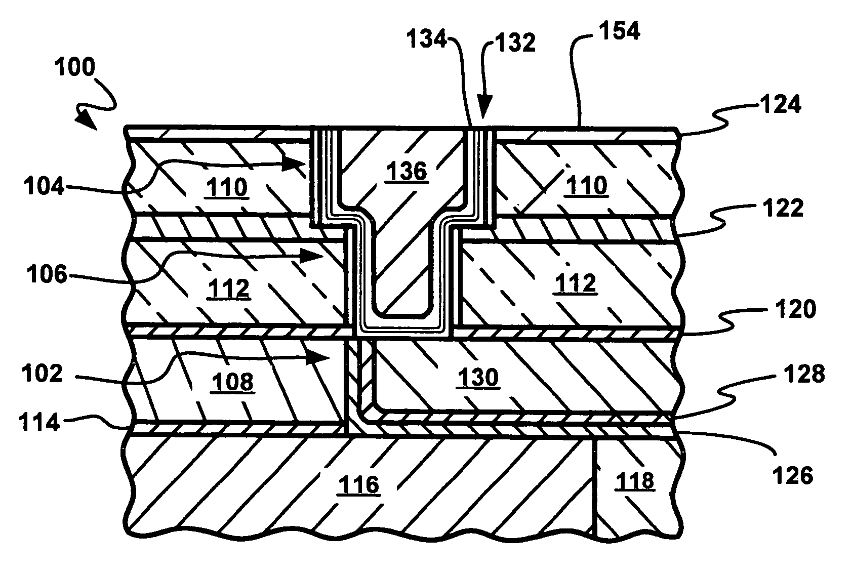
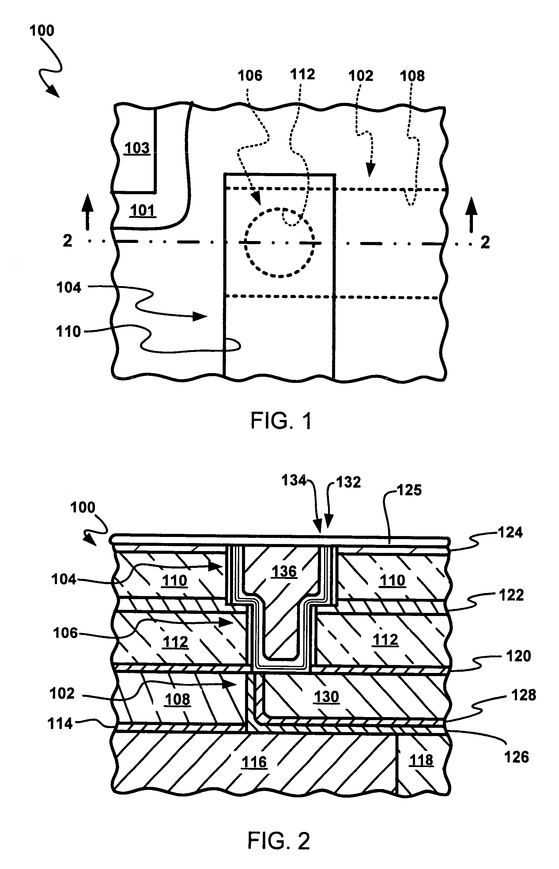
[0042]Referring now to FIG. 1, therein is shown a plan view of a semiconductor wafer 100 with a silicon semiconductor substrate 101 having semiconductor devices 103 formed thereon. Above the semiconductor substrate 101 in various dielectric layers are first and second channels 102 and 104 connected by a via 106. The first and second channels 102 and 104 are respectively disposed in first and second channel dielectric layers 108 and 110. The via 106 is an integral part of the second channel 104 and is disposed in a via dielectric layer 112. The semiconductor wafer 100 is shown without a capping layer, which will be discussed later.

[0043]The term “horizontal” as used in herein is defined as a plane parallel to the conventional plane or surface of a wafer, such as the semiconductor wafer 100, regardless of the orientation of the wafer. The term “vertical” refers to a direction perpendicular to the horizontal as just defined. Terms, such as “on”, “above”, “below”, “side” (as in “sidewal...


PUM


Abstract

An integrated circuit having a substrate and a semiconductor device thereon. A stop layer over the substrate has a first dielectric layer formed thereon having an opening into which a first conformal barrier is formed. A first conformal barrier liner is formed in the opening, processed, and treated to improve adhesion. Portions of the first conformal barrier liner on the sidewalls act as a barrier to diffusion of conductor core material to the first dielectric layer. A conductor material is formed in the opening over the vertical portions of the first conformal barrier liner and the first stop layer.

Description

CROSS-REFERENCE TO RELATED APPLICATION[0001]This is a Divisional of application Ser. No. 10 / 165,510 filed Jun. 6, 2002 now U.S. Pat. No. 6,657,304.[0002]The present application contains subject matter related to copending U.S. patent application Ser. No. 10 / 079,515 by Christy Mei-Chu Woo, John E. Sanchez, Darrell M. Erb, and Amit P. Marathe entitled “COPPER INTERCONNECT WITH IMPROVED BARRIER LAYER”. The related application is assigned to Advanced Micro Devices, Inc.TECHNICAL FIELD[0003]The present invention relates generally to semiconductor technology and more particularly to an integrated circuit interconnect.BACKGROUND ART[0004]In the manufacture of integrated circuits, after the individual devices such as the transistors have been fabricated in and on the semiconductor substrate, they must be connected together to perform the desired circuit functions. This interconnection process is generally called “metallization” and is performed using a number of different photolithographic,...

Claims


Application Information

Patent Timeline
IPC IPC(8): H01L23/52H01L21/3205H01L21/768
CPCH01L21/32051H01L21/76826H01L21/76829H01L21/76843H01L21/76871H01L21/76876H01L21/76831H01L2221/1089
Inventor WOO, CHRISTY MEI-CHUNGO, MINH VANSANCHEZ, JR., JOHN E.AVANZINO, STEVEN C.
Owner INNOVATIVE FOUNDRY TECH LLC
Why Eureka
Try Eureka