Unlock instant, AI-driven research and patent intelligence for your innovation.

Liquid crystal display and data latch circuit

a data latch and display technology, applied in static indicating devices, non-linear optics, instruments, etc., can solve the problems of disadvantageous increase of electric current consumption of sampling latch circuits b>5/b>, and the display resolution cannot be set too high, so as to achieve low power consumption and reduce power consumption

Inactive Publication Date: 2006-01-24
KK TOSHIBA
View PDF7 Cites 18 Cited by
  • Summary
  • Abstract
  • Description
  • Claims
  • Application Information

AI Technical Summary

Benefits of technology

This solution simplifies the signal line drive circuit structure, reduces power consumption, and enables higher display resolution by sharing latch circuits and converters, stabilizing operation and minimizing external voltage requirements.

Problems solved by technology

However, in case of the structure shown in FIG. 1, since the number of the sampling latch circuits 5, the load latch circuits 6 and the D / A converters 7 must be also increased as the display resolution becomes higher, there is a problem that the display resolution can not be set too high.
Consequently, a passing electric current flows from the power supply voltage terminal VDD toward a ground terminal VSS, and the electric current consumption of the sampling latch circuit 5 disadvantageously becomes large.

Method used


Image

  • Liquid crystal display and data latch circuit
  • Liquid crystal display and data latch circuit
  • Liquid crystal display and data latch circuit

Examples


first embodiment

[0071](First Embodiment)

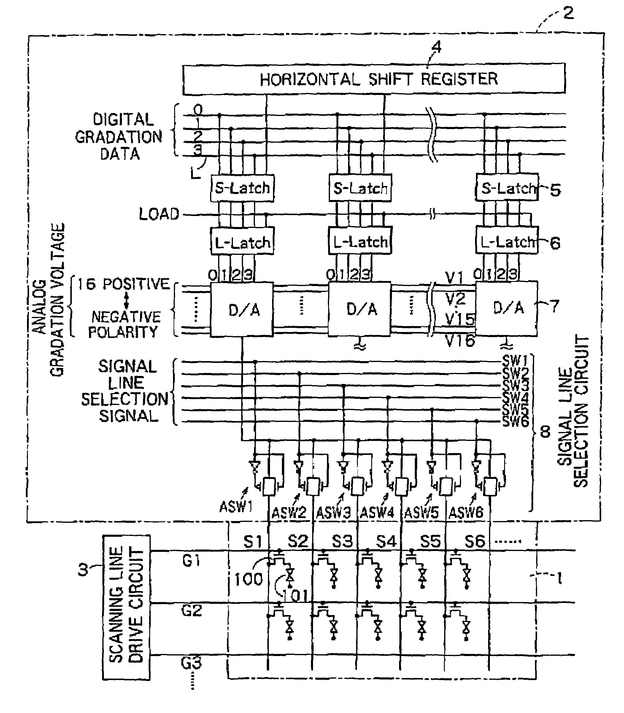
[0072]FIG. 5 is a block diagram showing a first embodiment of a liquid crystal display according to the present invention. The liquid crystal display FIG. 5 is characterized in that a latch circuit and a D / A converter are provided for every signal lines and they are commonly used, thereby reducing the number of the latch circuits and the D / A converters in the signal line drive circuit.

[0073]In general, it is known that the orientation of the liquid crystal is fixed to dull up operation of the liquid crystal and the darkish display is obtained when a voltage is applied to a liquid crystal layer constantly in the same direction. Thus, there is proposed a liquid crystal display adopting an alternating drive system such as V-line inversion driving by which the polarity of a voltage applied to the liquid crystal layer is switched in accordance with each vertical line as shown in FIG. 6A or HV-inversion driving by which the polarity of the voltage is switched in un...

second embodiment

[0106](Second Embodiment)

[0107]A second embodiment is a concrete example of the first embodiment, and shows an example in which a liquid crystal display having the display resolution of the 16-gradation QCIF standard (144×176 pixels) is constituted.

[0108]FIG. 9 is a block diagram of the second embodiment of the liquid crystal display according to the present invention and shows a structure of a signal line drive circuit 2. The signal line drive circuit 2 in the second embodiment includes a horizontal shift register 4, a sampling latch circuit 5a having a level conversion circuit, a load latch circuit 6, a gradation selection portion 11, and a signal line selection portion 12.

[0109]A protective diode 13 and a level conversion circuit (L / S, first level conversion circuit) 14 are connected between the horizontal shift register 4 and external input terminals XSTU, / XSTU, XCKU, and / XCKU. This level conversion circuit 14 converts the level of each signal inputted to the external input ter...

third embodiment

[0133](Third Embodiment)

[0134]A third embodiment is characterized in that a passing electric current does not flow from a power supply voltage terminal VDD to a ground terminal VSS in a sampling latch circuit 5.

[0135]FIG. 17 is a circuit diagram of a third embodiment of the sampling latch circuit 5. The sampling latch circuit 5 depicted in FIG. 17 includes a memory circuit 120 consisting of two inverters (first and second inverters) 121 and 122 each having an output terminal and an input terminal connected in the loop form, transistors (first and second switch devices) 123 and 124 for switching and controlling whether the power supply voltage VDD and the ground voltage VSS are to be supplied to each of these inverters, transistors (third switch devices) 125 and 126 for switching and controlling whether digital gradation data is to be supplied to the memory circuit 120, and NOR circuits (output circuits, first and second logic operation circuits) 127 and 128 for supplying data stored...


PUM


Abstract

A liquid crystal display in which a structure of a signal line drive circuit can be simplified is provided.The liquid crystal display according to the present invention includes sampling latch circuits, load latch circuits and D / A converters which are ⅙ of an aggregate number of signal lines, and drives every six signal lines for six times. As a result, a mounting area of a signal line drive circuit can be reduced. Further, after driving odd-numbered signal lines in a first half of a one-horizontal-line period, even-numbered signal lines are driven in a last half of the same. Therefore, V-inversion driving can be easily realized by only switching the polarity of an analog gradation voltage in the first half and the last half of the one-horizontal-line period. That is, since the number of times of switching the voltage polarity can be reduced, voltage control is facilitated, thereby hardly being influenced by noises. Furthermore, gradation power supply wirings for the positive polarity and gradation power supply wirings for the negative polarity required in the prior art, but the number of these wirings can be reduced by half, thereby decreasing a wiring area.

Description

CROSS REFERENCE TO RELATED APPLICATIONS[0001]This application claims benefit of priority under 35USC § 119 to Japanese Patent Application No. 2000-158365, filed on May 29, 2000, the entire contents of which are incorporated by reference herein.BACKGROUND OF THE INVENTION[0002](i) Field of the Invention[0003]The present invention relates to liquid crystal display for converting digital gradation data supplied from outside into an analog gradation voltage in an array substrate to drive signal lines and more particularly to a technique for forming a signal line drive circuit on an array substrate.[0004](ii) Description of the Related Art[0005]In general, an active matrix type liquid crystal display has a liquid crystal layer sandwiched and sealed between an array substrate and an opposed substrate, The array substrate includes a plurality of pixel electrodes arranged in the matrix form, a plurality of scanning lines arranged in a line direction along these pixel electrodes, a plurality...

Claims


Application Information

Patent Timeline
Patent Type & Authority Patents(United States)
IPC IPC(8): G09G3/36
CPCG09G3/3688G09G3/3614G09G2310/0294G09G2310/0289G09G2310/027G09G3/36
Inventor MORITA, TETSUO
Owner KK TOSHIBA