Multi-layer highly reflective ohmic contacts for semiconductor devices

Inactive Publication Date: 2006-01-31
LUMILEDS
View PDF28 Cites 117 Cited by
  • Summary
  • Abstract
  • Description
  • Claims
  • Application Information

AI Technical Summary

Benefits of technology

[0007]In an alternate embodiment, a barrier layer interposes the ohmic and reflector layers to prevent any unwanted device-degrading inter-metallics ...

Problems solved by technology

Therefore, because of reliability issues, Ag is us...

Method used


Image

  • Multi-layer highly reflective ohmic contacts for semiconductor devices
  • Multi-layer highly reflective ohmic contacts for semiconductor devices
  • Multi-layer highly reflective ohmic contacts for semiconductor devices

Examples


Embodiment Construction

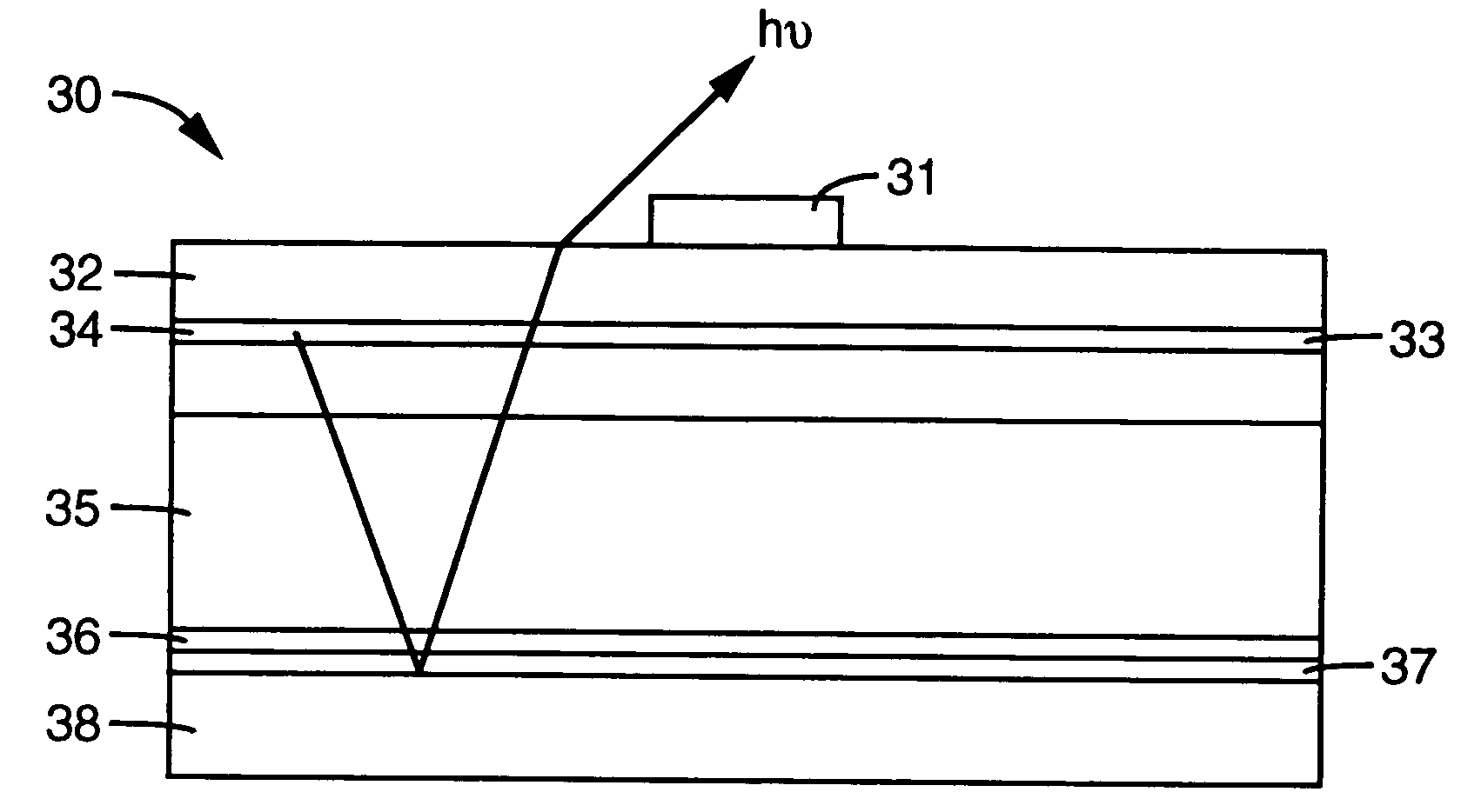
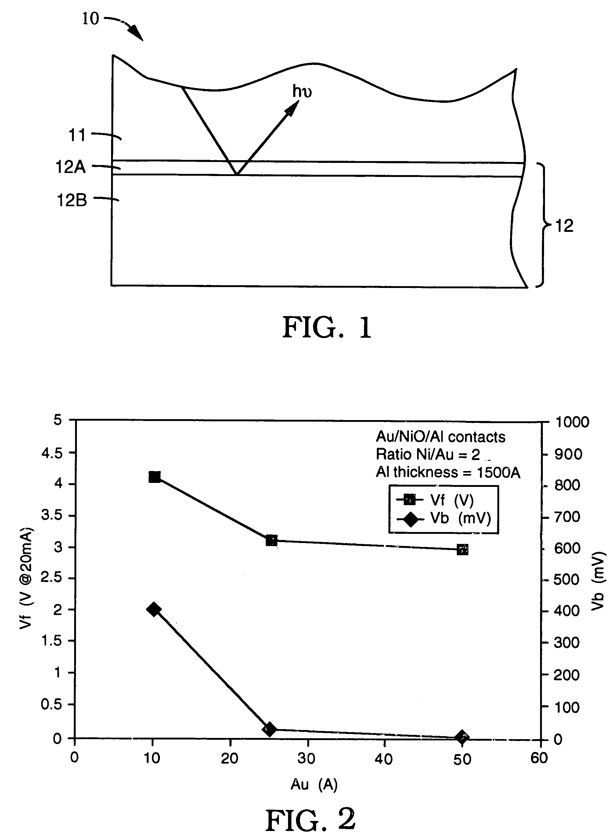
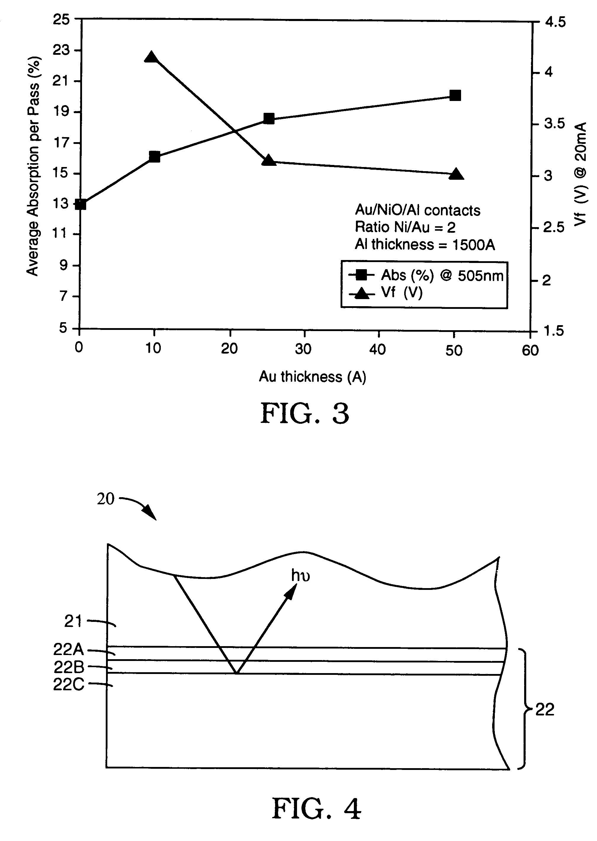
[0014]The present invention is a multi-layer contact that consists of multiple material layers providing high reflectivity, low specific contact resistance, and high reliability. FIG. 1 shows a cross-sectional embodiment of a semiconductor device 10 with a multi-layer contact 12. The multi-layer contact 12 includes an ohmic layer 12A and a reflective layer 12B. In combination, the ohmic and reflective layers 12A, 12B form a highly reflective ohmic electrical contact to semiconductor structure 11. Various optoelectronic semiconductor structures 11 can be used with the multi-layer reflective contact layers 12. Symbol hν in FIG. 1 designates the path of a photon reflected by multi-layer contact 12.

[0015]Ohmic layer 12A is at least one layer that provides a good ohmic contact to the semiconductor 11. A good ohmic contact has minimal voltage drop (linear I-V, where “I” is current and “V” is voltage) across the semiconductor / metal interface when current flows across it. A figure of merit ...


PUM


Abstract

A high performance, highly reflective ohmic contact, in the visible spectrum (400 nm–750 nm), has the following multi-layer metal profile. A uniform and thin ohmic contact material is deposited and optionally alloyed to the semiconductor surface. A thick reflector layer selected from a group that includes Al, Cu, Au, Rh, Pd, Ag and any multi-layer combinations is deposited over the ohmic contact material.

Description

FIELD OF THE INVENTION[0001]This invention relates to electrical contacts on optoelectronic devices such as light-emitting diodes (LEDs).BACKGROUND[0002]Optoelectronic devices such as light-emitting diodes (LEDs) emit light in response to an excitation signal. A typical LED is a heterostructure that has been deposited on a host substrate via a growth technique such as liquid phase, hydride phase, molecular beam, and metal-organic phase epitaxy. The heterostructure includes n and p-type semiconductor layers that sandwich active light producing layers. Electrical contacts are attached to the n and p-type semiconductor layers. When a forward voltage is applied across the contacts, electrons and holes are injected from the n and p-type semiconductor layers into the active region. Light is produced when the electrons and holes radiatively recombine in the active layer(s).[0003]Wall-plug efficiency is the amount of light power produced compared to the electrical power applied. High wall-p...

Claims


Application Information

Patent Timeline
IPC IPC(8): H01L33/00H01L33/40
CPCH01L33/405
Inventor WIERER, JR., JONATHAN J.KRAMES, MICHAEL RRUDAZ, SERGE L
Owner LUMILEDS
Why Eureka
Try Eureka