Electronic package having a thermal stretching layer

Inactive Publication Date: 2006-01-31
GLOBALFOUNDRIES US INC
View PDF13 Cites 35 Cited by
  • Summary
  • Abstract
  • Description
  • Claims
  • Application Information

AI Technical Summary

Benefits of technology

[0009]According to one aspect of the invention, there is provided an electronic package comprising a circuitized substrate including a first surface with a first and second portion thereon, the substrate having a first stiffness, a plurality of electrically conductive circuit members positioned on the first portion of the first surface of the circuitized substrate, each of the plurality of electrically conductive circuit members adapted for having solder connections thereon and for being electrically connected to a semiconductor chip, and a stiffener layer having a second stiffness positioned on the second portion of the first surface relative to the first portion, the second stiffness of the stiffener layer distributing a portion of the first stiffness of the circuitized substrate so as to substantially prevent failure of the solder connections between the electrically conductive circuit members and the semiconductor chip during operation of the electronic package.
[0010]According to another aspect of the invention, there is provided a method of making an electronic package comprising the s

Problems solved by technology

During these temperature changes, a spatial distribution of coefficient of thermal expansion (CTE) in the chip carrier coupled with the compliancy of the chip carrier, may cause the chip carrier to bow (or flex) upward or downward and thus deviate from planarity.
Unfortunately the stiffener ring assembly with bonding adhesive acts as a mechanical clamp on the outer perimeter of the organic chip carrier that constrains outer portions of the chip carrier from expanding, particularly when subjected to elevated and varying temperature.
This constraint can occur during processing and usage, even if the thermal expansion coefficients of the stiffener ring and the organic chip carrier are matched, due to temperature gradients within the chip carrier which can cause expansion mismatches.
An adverse consequence of chip carrier bowing during build and operation of the chip carrier, particularly when a bonded stiffener ring is used with a compliant organic chip carrier, can be unreliable decoupling

Method used


Image

  • Electronic package having a thermal stretching layer
  • Electronic package having a thermal stretching layer
  • Electronic package having a thermal stretching layer

Examples


Example

[0019]In the following description, like numerals will be used to identify like elements.

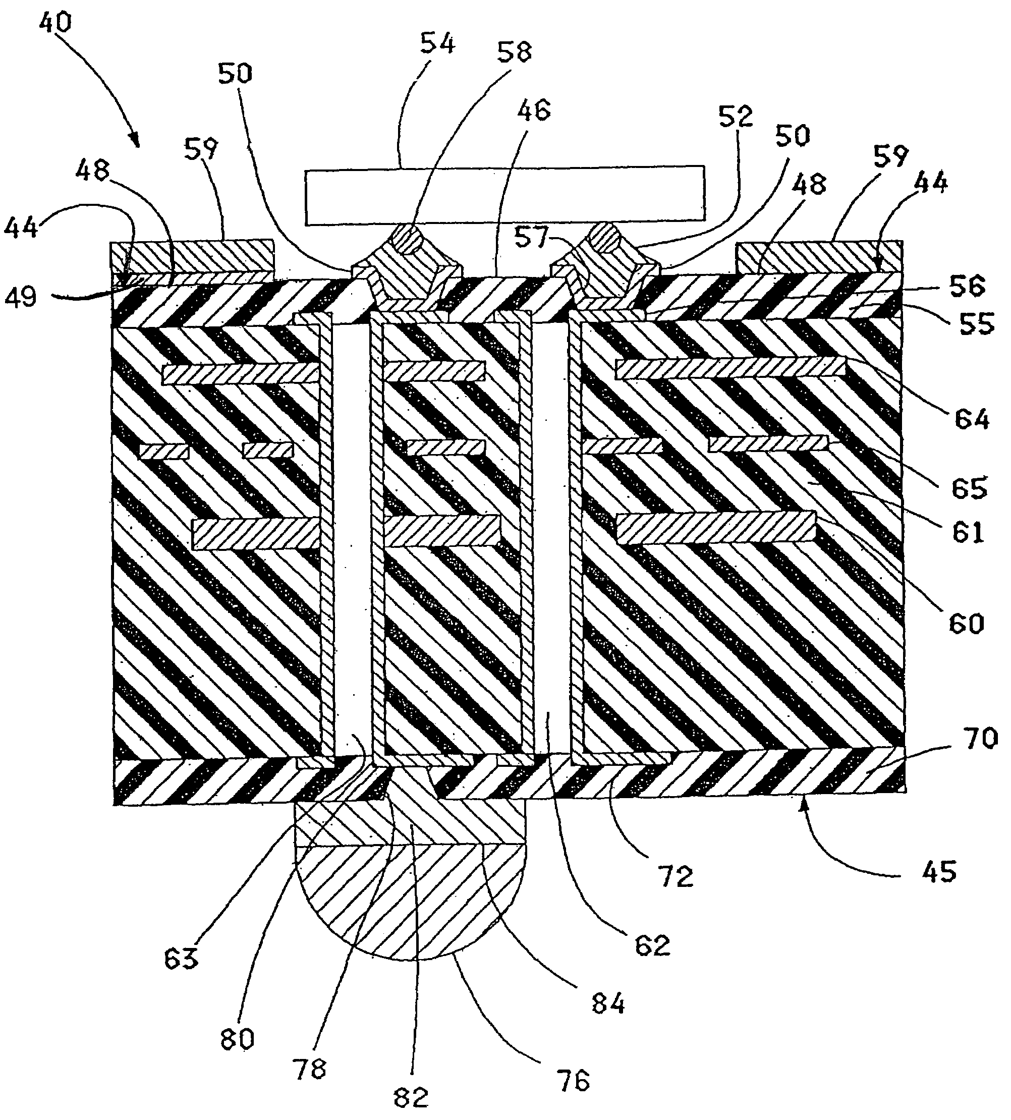
[0020]Referring to FIG. 3, a partial sectional view in elevation of one embodiment of the electronic package 40 of the invention is shown. Electronic package 40 includes a circuitized substrate 42, preferably an organic chip carrier, having a first surface 44 with a first portion 46 and a second portion 48 thereon. Circuitized substrate 42 includes a second surface 45. The circuitized substrate has a first stiffness from about 0.1 Mpsi to about 10 Mpsi. The first stiffness is an overall measure of the average stretching stiffness (in-plane stiffness) through the entire thickness of circutized substrate 42. The first stiffness will be described in more detail below. Circuitized substrate 42 includes a plurality of electrically conductive circuit members 50 positioned on first portion 46 of first surface 44. The electrically conductive circuit members are preferably comprised of a metal, the metal...


PUM


Abstract

An electronic package and method of making same in which a circuitized substrate having a first stiffness includes a plurality of electrically conductive circuit members on a first portion of the circuitized substrate and is adapted for having solder connections thereon and for being electrically connected to a semiconductor chip. A stiffener layer having a second stiffness is positioned on a second portion of the circuitized substrate relative to the first portion, the second stiffness of the stiffener layer distributing a portion of the first stiffness of said circuitized substrate so as to substantially prevent failure of the solder connections between the electrically conductive circuit members and the semiconductor chip during operation of the electronic package.

Description

TECHNICAL FIELD[0001]The present invention relates to an electronic package for making electrical interconnection between a circuitized substrate and a semiconductor chip; more particularly, the electronic package includes a stiffener layer that substantially prevents failure of electrical interconnections between the electronic package and the semiconductor chip during manufacture and operation.BACKGROUND OF THE INVENTION[0002]A semiconductor chip may be mechanically and electrically interconnected to a circuitized substrate (e.g., a circuit board) of an electronic package, such as a chip carrier, by having conductive contacts on the chip (e.g., solder balls) solderably coupled to electrically conductive circuit members on the top surface of the chip carrier. For example, there may be large metal pads, such as copper pads, on the bottom of the chip carrier to accommodate a ball grid array of solder balls for coupling the chip carrier to a circuit card, and smaller amounts of metal ...

Claims


Application Information

Patent Timeline
IPC IPC(8): H01L23/053H05K1/03H01L23/00H01L23/373H05K1/02H05K1/11H05K3/46
CPCH01L23/3735H05K1/0271H01L23/562H01L2924/01322H01L2224/16H01L2924/01025H01L2924/01079H01L2924/15311H01L2924/3011H01L2924/3025H01L2924/3511H05K1/0203H05K1/112H05K3/4602H05K2201/09781H05K2201/10674H05K2201/2009H05K1/02
Inventor ALCOE, DAVID J.LI, LISATHE, SANJEEV B.
Owner GLOBALFOUNDRIES US INC
Why Eureka
Try Eureka