Drive circuit, display device, and driving method

a technology of drive circuit and display device, which is applied in the direction of static indicating device, cathode-ray tube indicator, instruments, etc., can solve the problems of difficult to realize this value, deformation or change in quality, and cracks in a portion of electro conductive thin film 3004 locally broken, so as to increase the driving energy for driving and reduce the current flowing in a moment

Inactive Publication Date: 2006-02-07
CANON KK
View PDF40 Cites 33 Cited by
  • Summary
  • Abstract
  • Description
  • Claims
  • Application Information

AI Technical Summary

Benefits of technology

[0046]According to the aspect of the present invention, the light-emitting device can be correctly driven by stepwise raising the driving waveform. When the rising portion of the driving waveform has a level higher than the level Ak, it is not desired to raise the driving waveform suddenly after the level Ak has been reached. Therefore, in the above mentioned aspect of the present invention, it is desired that the level Ak is the maximum level of the driving waveform (at least in the rising portion).
[0112]According to the driving method of the present invention, a combination use of pulse width control and pulse level control enables the resolution of a level of pulse level control, that is, the minimum level difference, to be set as an easily realized value. Furthermore, the resolution of the pulse width control, that is, the slot width can be larger to lower the maximum frequency of a drive signal and the maximum level. Especially, by raising or dropping the driving waveform in a stepped form, the levels of the rising or falling portions can be protected against a sudden change. Thus, for example, an unnecessary radiation can be suppressed. Furthermore, an irregular driving waveform can be reduced to prevent the deterioration of the gray-scale characteristic at a low gray scale level. In addition, the occurrence of overshoot or ringing can be suppressed, and the application of an abnormal voltage to a light-emitting device can be prevented.

Problems solved by technology

In addition, a crack arises in a portion of the electro conductive thin film 3004 which is locally broken, deformed or changed in quality.
In addition, even if plenty of devices are arranged in high density on a substrate, it is seldom to generate problems such as a thermofusion of a substrate.
It is difficult to realize this value when considering characteristics of an IC, a printed circuit board, and a power supply which constitute a drive circuit.
That is, since a level of a driving waveform which consists of only high frequency spectrum components, that is, a pulse width modulation driving waveform at low gradation becomes low, it is not possible to display an image at desired gradation in a low gradation region.
In addition, even when a long pulse is supplied, the drive current If which flows into an electron emission device becomes a waveform with large leading time.
Although a cold cathode type electron emission device itself has high-speed responding capability, a current waveform supplied to the electron emission device becomes dull, and hence, a waveform of an emission current Ie is also deformed as a result.
In addition, as for voltage drive, there are the following troubles to be solved.
If a conventional voltage driving method is applied to such a circuit, since a charging current i flows into a parasitic capacitance by the application of a voltage, a leading edge of a driving waveform becomes dull.
Furthermore, by a self-induction action of the parasitism inductance, electromotive force U=—Lx(di / dt) arises, overshoot and ringing arise, and the application of an abnormal voltage to a light emitting device arises.
In recent years, demand for display units with a large area, high resolution, and fine gradation has been remarkable, parasitic inductance and parasitic capacitance of wiring have increased in connection with it, and hence, elimination of gradations in a low luminance brightness region which is caused by dullness, an overshoot, and ringing of a leading edge of a driving waveform have become increasingly important problems to be solved.
In addition, it has become a problem that it becomes impossible that a driving waveform by simple pulse width control and pulse height value control guarantees the monotonicity of gradation because of changes and dispersion of voltage / luminescence intensity characteristics of light emitting devices.
However, in the drive by the conventional pulse width modulation, there is a further possibility of inducing large electromagnetic wave noise, i.e., the spurious radiation of an electromagnetic wave at leading and trailing edges of a driving waveform depending on gradation.
In addition, in a multi-electron beam source where many electron emission devices described above are arranged in a matrix, there is a problem that a voltage applied to each device becomes smaller as the device is apart from its feeding terminal due to a voltage drop caused by an influence of its wiring resistance, and in consequence, the discharge electron distribution of each device does not become uniform.
Then, when this multi-electron emission device is applied to an image display unit, there is a problem that image quality deteriorates due to a voltage drop caused by a wiring resistor.
In addition, when a pixel count increases and the current which flows into a selection electrode increases, the voltage dispersion becomes large.
This appears as the difference of luminance brightness between pixels which are elements which emit light by an electron beam emitted from its electron emission device, and leads to the degradation of display quality as an image display unit.

Method used


Image

  • Drive circuit, display device, and driving method
  • Drive circuit, display device, and driving method
  • Drive circuit, display device, and driving method

Examples


example 1

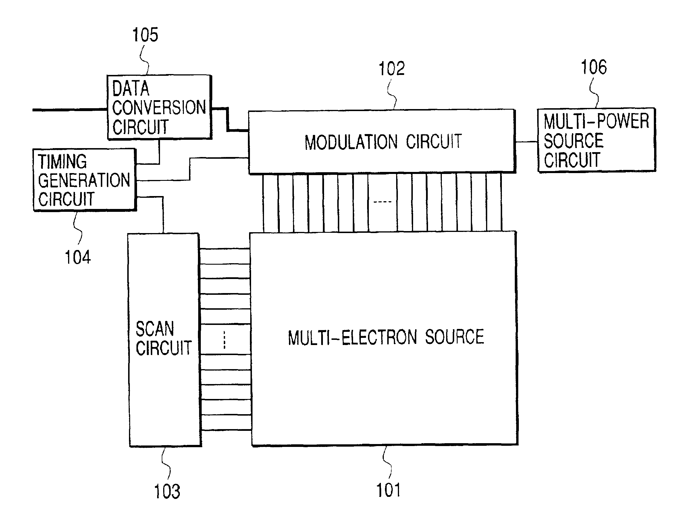
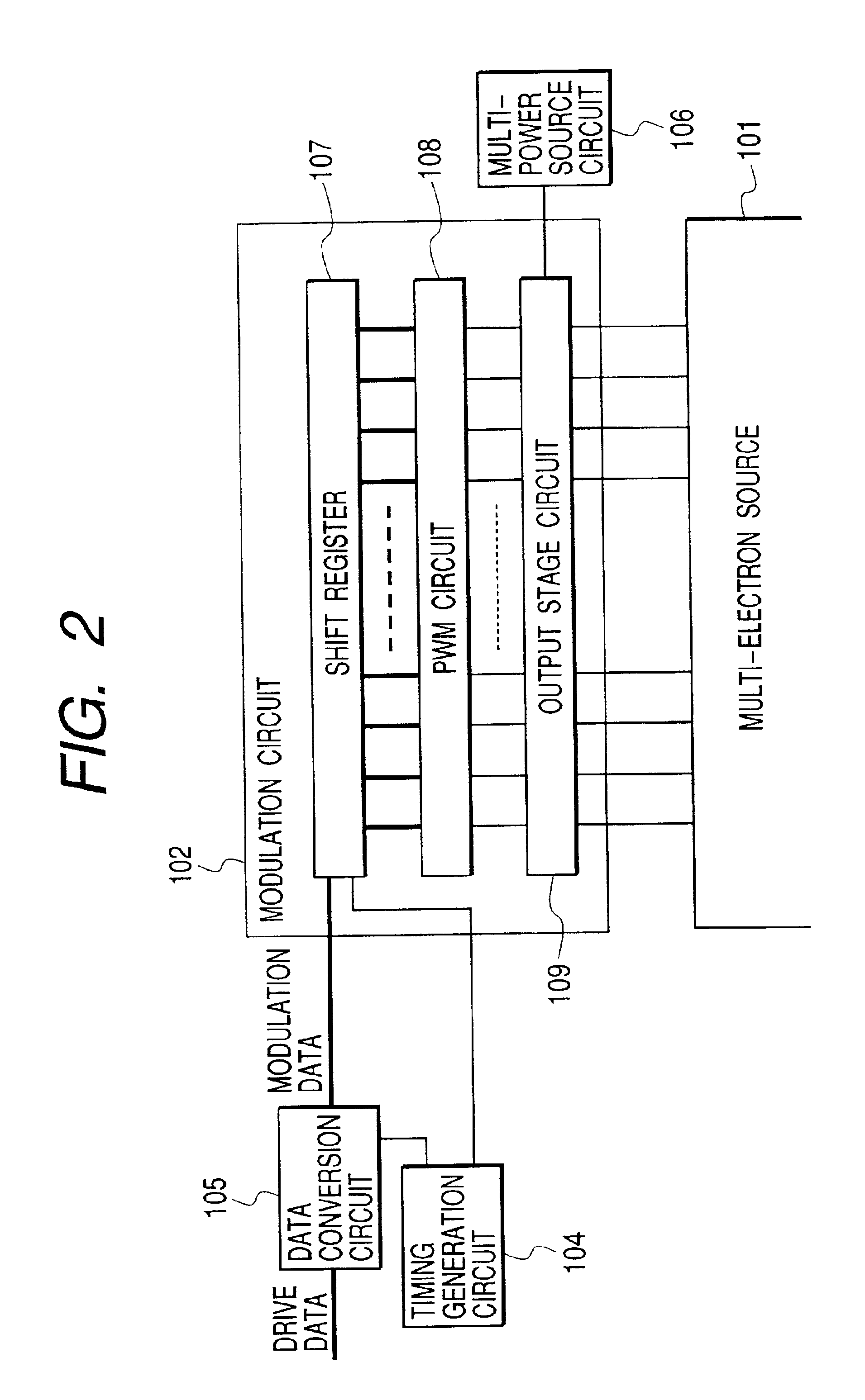
[0159]FIG. 1 is a block diagram of a multi-electron source drive circuit according to an example of the present invention. This figure shows a multi-electron source 101, a modulation circuit 102, a scan circuit 103, a timing generation circuit 104, a data conversion circuit 105, and a multi-power source circuit 106. A multi-electron source 101 is driven in this structure. As shown in FIG. 34, the multi-electron source 101 comprises an electron source (electron emission device) 1 provided in an intersection of row-directional wiring 2 and column-directional wiring 3. As an electron source, although the SCE type, FE type, and MIM type electron emission device are known as described above, in this Example, the SCE type electron emission device was used.

[0160]The data conversion circuit 105 converts drive data, used for driving the multi-electron source 101 from the external, into a format suitable for the modulation circuit 102. The modulation circuit 102 is connected to the column-dir...

example 2

[0185]FIG. 18 shows another example of V14 waveforms. Driving waveforms in FIG. 7 show an example in the case of setting respective drive level potentials V1, V2, V3, and V4 so that a ratio of luminescence intensity might be set to 1:2:3:4. In an LED or an electron emission device, since luminescence intensity is proportional to a drive current in general, hereafter, this is called a current equal dividing method. On the other hand, FIG. 19 shows the case that it is determined to make a ratio of V1, V2, V3, and V4 be 1:2:3:4, i.e., to make potential differences V4−V3, V3−V2, V2−V1, and V1−V0 (reference potential V0 of a driving waveform was made the same as a drive threshold of a device also here) fixed, and hereafter, this is called a voltage equal dividing method. FIG. 19 shows the voltage / current (luminescence intensity) in the voltage equal dividing method.

[0186]In FIG. 18, a reverse unit driving waveform block in an N-th gradation denotes differential from a (N−1)-th gradation....

example 3

[0190]FIG. 21 shows an example of Vn driving waveforms. This waveform is for performing driving with a waveform where a level of a driving waveform of data N is made to be k (k is an integer that is one or more, and less than n) when luminance brightness data consists of R bits and luminance brightness data is approximately 0R) (k / n−1). In the driving waveform in FIG. 8, if the number of unit drive blocks (the number of slots) of the level k of the driving waveform in an (n−1)-th gradation becomes 3 by adding a unit drive block to a driving waveform in an (n−2)-th gradation when a level k is three or less, a unit drive block with a level of k+1 is added to a driving waveform in the following n-th gradation. However, in driving waveforms in FIG. 21, a level (level) is not carried until the number of unit drive blocks with a level of 1 (level 1; the minimum level) reaches a predetermined maximum number S (in this Example, 259) when increasing gradation, but when the number reaches the...


PUM


Abstract

A drive waveform signal which is level controlled by discontinuous levels including a minimum level corresponding to luminance brightness gradation data which is not 0, at least one non-minimum level corresponding to larger luminance brightness gradation data, and an intermediate level between the minimum and non-minimum level. The signal, which is employed to drive an image display unit, is given pulse width control with discontinuous pulse width, and has a portion, controlled with the minimum level, in its trailing edge, and a portion, controlled with the intermediate level just before the former portion, when it has the portion controlled by the non-minimum level.

Description

BACKGROUND OF THE INVENTION[0001]1. Field of the Invention[0002]The present invention relates to a drive circuit for generating a driving waveform corresponding to brightness data; a display device therewith; a driving method for generating the driving waveform; and more specifically to a method of driving a light-emitting device in an image display device provided with an image display panel having the matrix wiring of a plurality of light-emitting devices.[0003]2. Related Background Art[0004]Up to now, two kinds of electron emission devices, that is, a hot cathode device and a cold cathode device are known. Among these, as a cold cathode device, for example, a surface conduction electron-emitting device, a field emission type device (hereafter, an FE type device), a metal / insulating film / metal type discharge device (hereafter, an MIM type device), etc. are known. As a surface conduction electron-emitting device, for example, a device disclosed in an article of “M. I. Elinson, Radi...

Claims


Application Information

Patent Timeline
Patent Type & Authority Patents(United States)
IPC IPC(8): G09G3/10G09G3/20G09G3/00G09G3/22G09G5/10
CPCG09G3/2011G09G3/22G09G3/2018G09G5/10G09G2310/06
Inventor AOKI, TADASHIKATAKURA, KAZUNORIISONO, AOJIMURAYAMA, KAZUHIKOSHINO, KENJI
Owner CANON KK
Why Eureka
Try Eureka