Providing an improved organic vertical cavity laser array device

a laser array and organic technology, applied in semiconductor lasers, optical resonator shapes and construction, active medium materials, etc., can solve the problems of degradation problems of organic materials, the density level (and pixel size) is far beyond the capabilities, and the only way to achieve high power densities, etc., to reduce scattering losses, increase power conversion efficiency, and reduce scattering losses

Inactive Publication Date: 2006-02-07
EASTMAN KODAK CO
View PDF9 Cites 9 Cited by
  • Summary
  • Abstract
  • Description
  • Claims
  • Application Information

AI Technical Summary

Benefits of technology

[0016]It is an advantage of the present invention to provide a way of making a two-dimensional organic laser array device employing micron-sized laser pixels which can be optically driven by large area sources and produce either single or multi-mode laser output, such that there is reduced scattering loss and increased power conversion efficiency. The devices employ a microcavity design incorporating high reflectance dielectric stacks for both the top and bottom reflectors; and have a gain media including organic material. The micron-sized laser pixels of the device are provided by modulating the reflectance of the bottom dielectric stack, where the modulation is obtained by etching the surface of the bottom dielectric stack. In order to reduce scattering losses and avoid depositing the active region and top dielectric stack over a non-planar surface, the etched surface is made planar by forming a planarization layer between the etched surface and the active region. As a result of planarizing the etched surface of the bottom dielectric stack, there is reduced scattering loss and increased power conversion efficiency for two-dimensional organic laser array devices.

Problems solved by technology

Such high power densities can only be achieved by using other lasers as the pump sources, precluding that route for inorganic laser cavities.
This power density level (and pixel size) is far beyond the capabilities of LED's and, additionally, would most likely cause some degradation problems with the organic materials if they were driven cw.
Unfortunately, broad-area laser devices having 350 μm diameter emitting areas would lead to highly multimode output and to lower power conversion efficiencies (as a result of filamentation).

Method used


Image

  • Providing an improved organic vertical cavity laser array device
  • Providing an improved organic vertical cavity laser array device
  • Providing an improved organic vertical cavity laser array device

Examples


Embodiment Construction

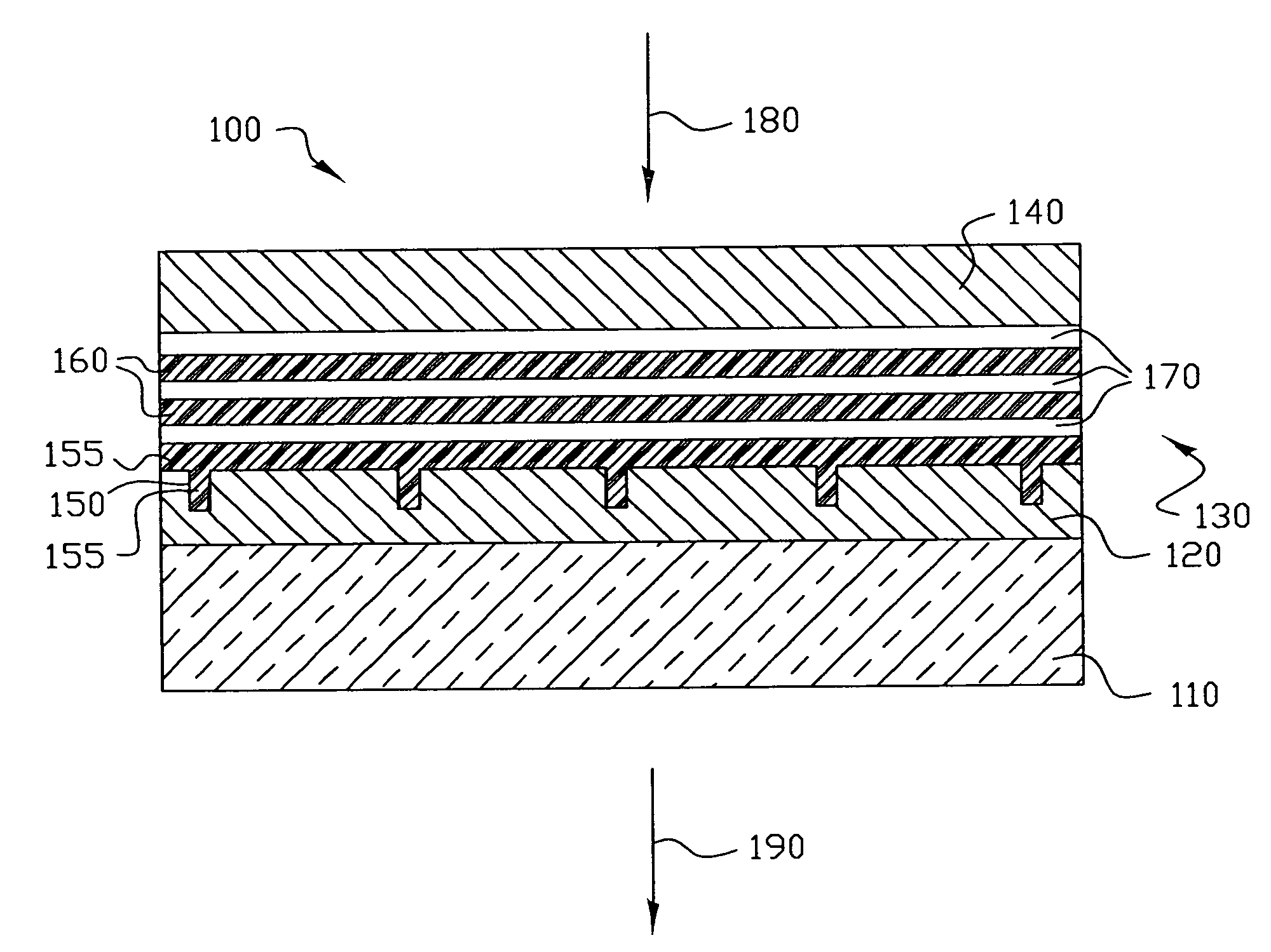
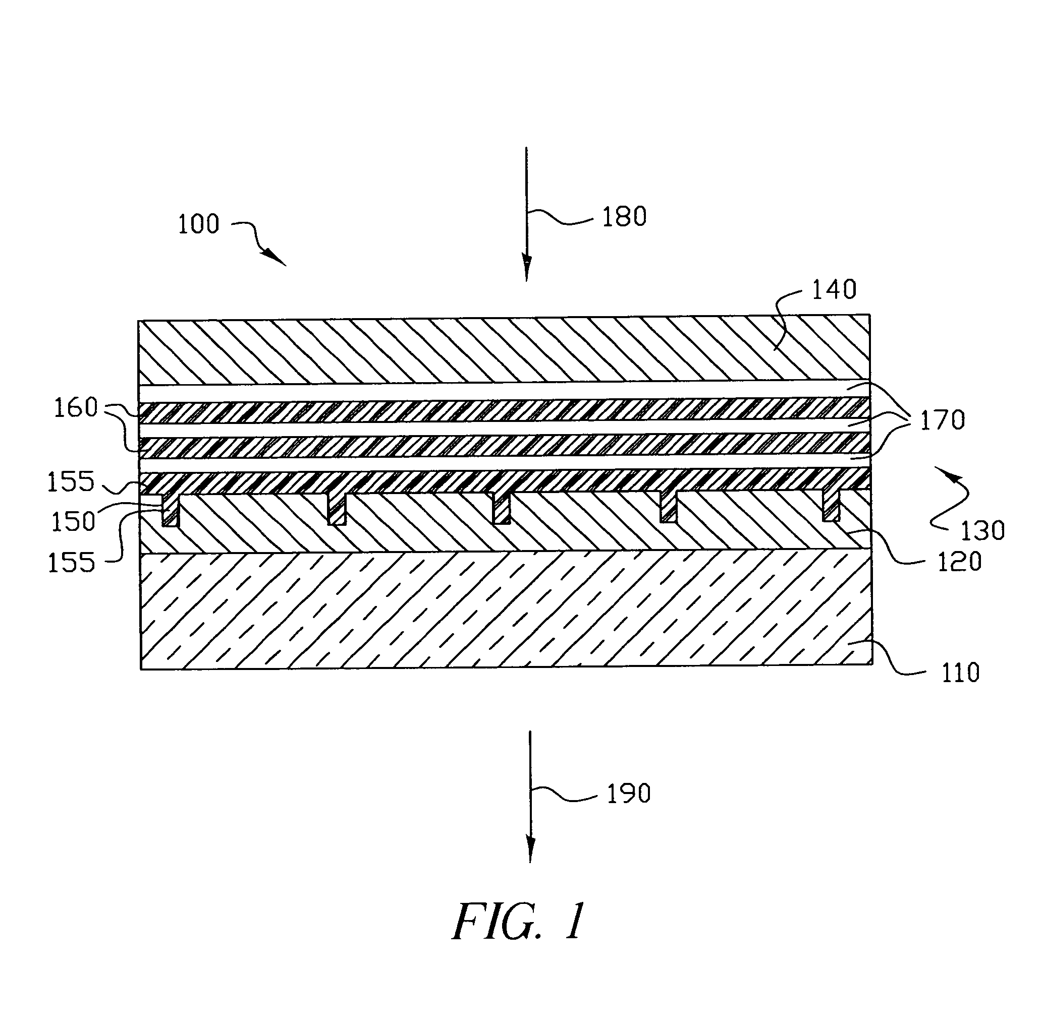
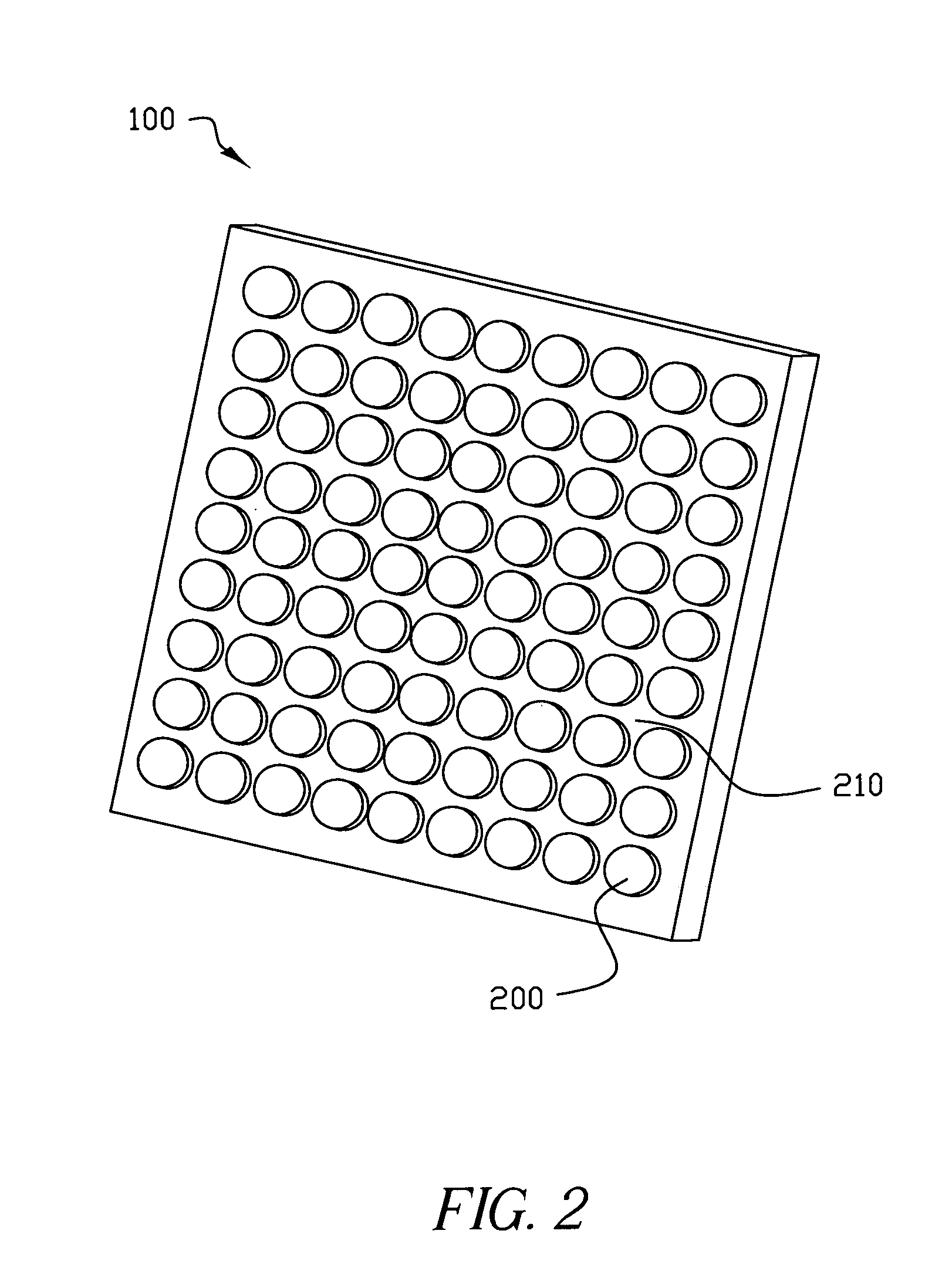
[0019]To enable a large area laser structure, which emits single-mode (or a few modes), it is necessary to construct a two-dimensional laser array device 100 as shown schematically in FIG. 1 and in accordance with the present invention. FIG. 2 shows a top-view of the two-dimensional laser array device 100 where on the surface of the VCSEL needs to be defined lasing pixels 200 separated by interpixel regions 210. If single mode lasing action is desired, then the emission from the various pixels needs to be phase-locked, i.e., intensity and phase information must be exchanged amongst the pixels. This is best obtained by weakly confining the laser emissions to the pixel regions by either small amounts of built-in index or gain guiding and arranging the pixels in a periodic two-dimensional array. For the laser pixels 200 arranged in a square two-dimensional array, phase-locked operation results in each element being 180 degrees out of phase with its four nearest neighbors (E. Kapon and ...


PUM


Abstract

A method of making an organic vertical cavity laser array device includes providing a substrate and a bottom dielectric stack reflective to light over a predetermined range of wavelengths and being disposed over the substrate; forming an etched region in the top surface of the bottom dielectric stack to define an array of spaced laser pixels which have higher reflectance than the interpixel regions so that the array emits laser light; and forming a planarization layer over the etched bottom dielectric stack. The method also includes forming an active region over the planarization layer for producing laser light; and forming a top dielectric stack spaced from the bottom dielectric stack and reflective to light over a predetermined range of wavelengths.

Description

CROSS REFERENCE TO RELATED APPLICATIONS[0001]This is a continuation-in-part of application Ser. No. 10 / 066,829 now U.S. Pat. No. 6,687,274 filed Feb. 4, 2002 entitled “Organic Vertical Cavity Phase-Locked Laser Array Device” by Keith B. Kahen.[0002]Reference is made to commonly assigned U.S. patent application Ser. No. 09 / 832,759 now U.S. Pat. No. 6,658,037 filed Apr. 11, 2000 by Keith B. Kahen et al.; U.S. patent application Ser. No. 10 / 066,936 now U.S. Pat. No. 6,674,776 filed Feb. 4, 2002 entitled “Organic Vertical Cavity Lasing Devices Containing Periodic Gain Regions” by Keith B. Kahen et al.; commonly assigned U.S. patent application Ser. No. 10 / 066,829 now U.S. Pat. No. 6,687,274 filed Feb. 4, 2002 by Keith B. Kahen et al., and commonly assigned U.S. patent application Ser. No. 10 / 609,922 now U.S. Pat. No. 6,790,696 filed concurrently herewith by Keith B. Kahen, the disclosures of which are incorporated herein by reference.FIELD OF THE INVENTION[0003]The present invention rel...

Claims


Application Information

Patent Timeline
Patent Type & Authority Patents(United States)
IPC IPC(8): H01S3/04H01S3/16H01S3/06H01S3/08H01S3/0933H01S5/36H01S5/42
CPCH01S3/0604H01S3/0627H01S3/08H01S5/423H01S3/168H01S5/36
Inventor KAHEN, KEITH B.DEBAR, MICHAEL J.SHANTHARAMA, LINGADAHALLI G.
Owner EASTMAN KODAK CO
Why Eureka
Try Eureka