Enhanced selectivity for epitaxial deposition

a selective deposition and epitaxial technology, applied in the direction of single crystal growth, semiconductor devices, chemistry apparatus and processes, etc., can solve the problems of unsuitable polycrystalline silicon on the gate, gate shortening to the elevated source and drain region,

Active Publication Date: 2006-02-14
ASM IP HLDG BV
View PDF55 Cites 72 Cited by
  • Summary
  • Abstract
  • Description
  • Claims
  • Application Information

AI Technical Summary

Benefits of technology

[0009]Thus, it is desired to develop improved methods for forming an elevated source/drain (“ESD”) structure. In particular, it is desired to selectively deposit a thin ep...

Problems solved by technology

Additionally, if a polycrystalline silicon gate is used, undesired polycrystalline silicon will form on the gate during monocrystalline silicon deposition on the source and drain substrate areas.
Excessive polycrystalline silicon deposition on the gate can cause the gate to short t...

Method used


Image

  • Enhanced selectivity for epitaxial deposition
  • Enhanced selectivity for epitaxial deposition
  • Enhanced selectivity for epitaxial deposition

Examples


Embodiment Construction

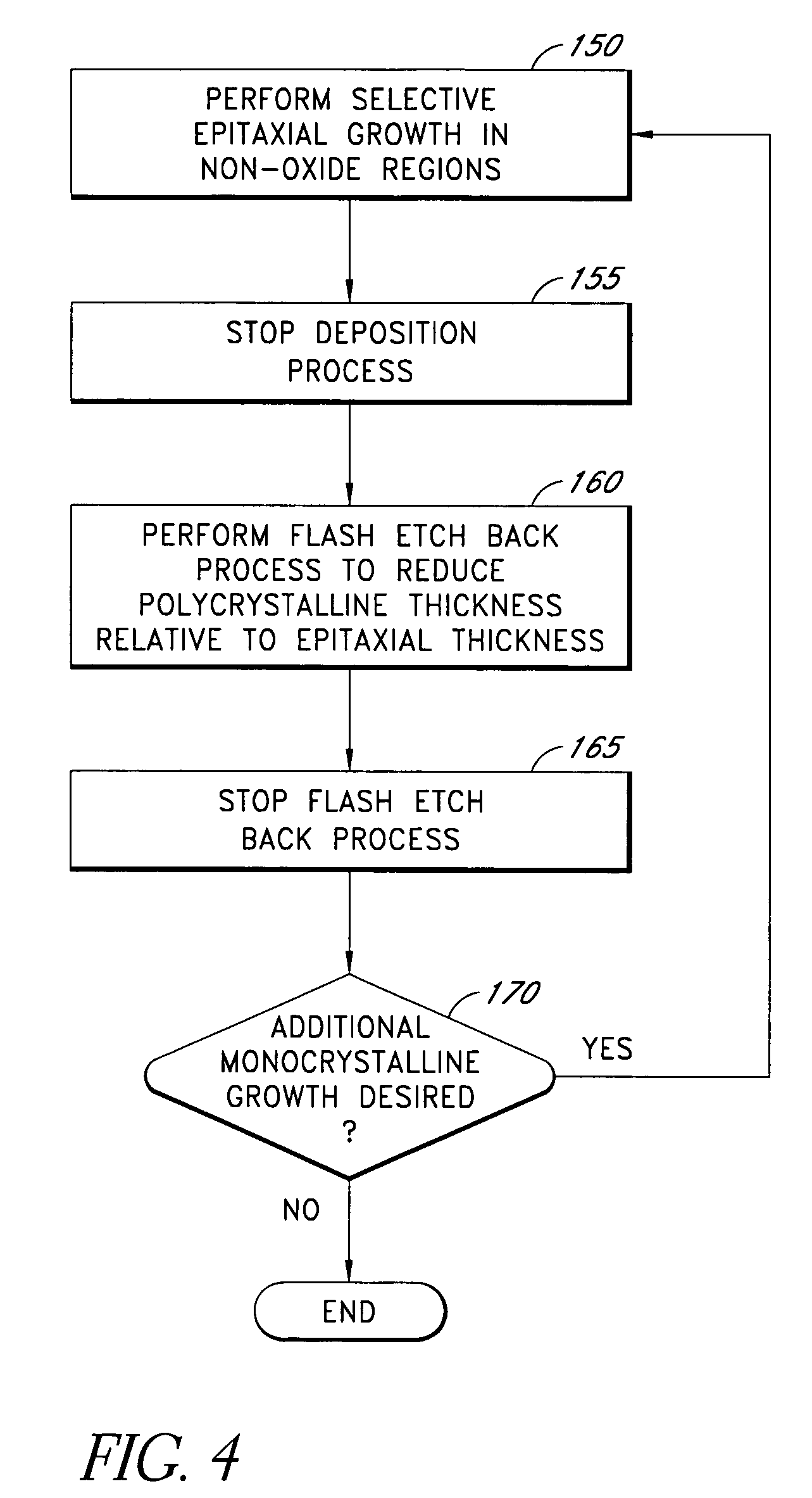
[0020]As expounded in detail below, the present disclosure provides methods of fabricating an improved ESD structure. In particular, the present disclosure provides methods for reducing unwanted polycrystalline silicon deposition on a gate region during formation of an elevated ESD structure. However, one of ordinary skill in the art will recognize that the methods disclosed herein also can be applied to any deposition process wherein epitaxial deposition is desired in a first region, while controlled non-epitaxial deposition at a different rate is desired in a second region. “Controlled” deposition, as used herein, means that the rate of deposition in the second region can vary from 0% to nearly 100% of the rate of epitaxial deposition in the first region.

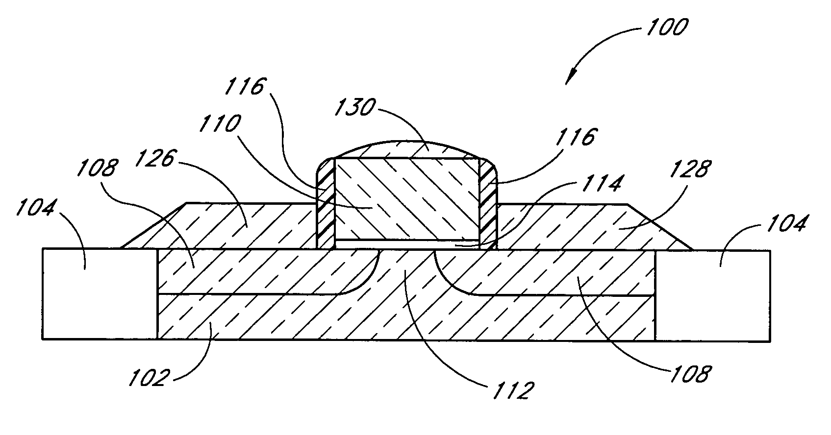
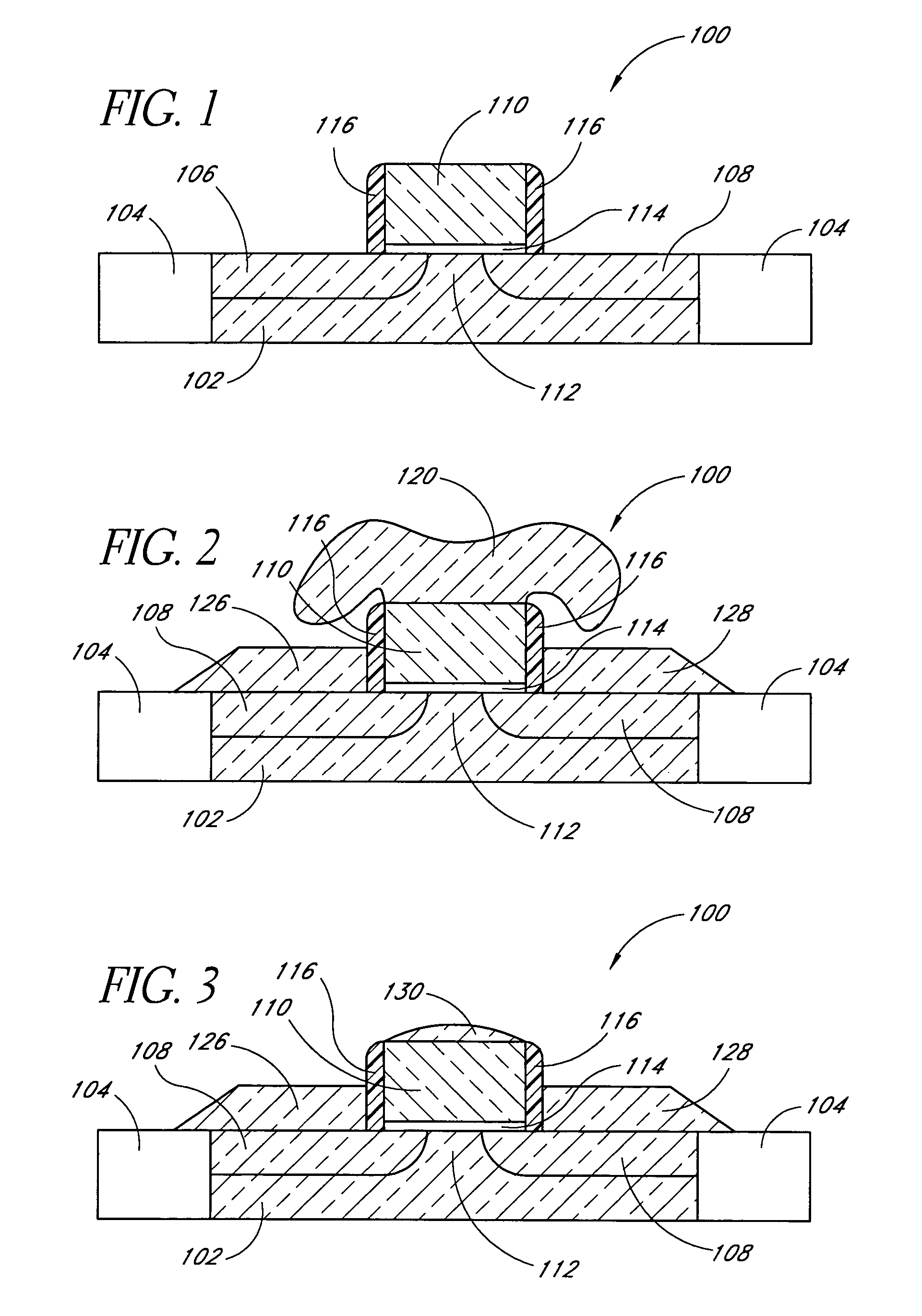
[0021]FIG. 1 illustrates the basic structure of a conventional field effect transistor 100. The field effect transistor 100 comprises a substrate 102 and shallow trench isolation regions 104. The substrate 102 is formed of any of ...


PUM


Abstract

A method of forming an electronic component having elevated active areas is disclosed. The method comprises providing a semiconductor substrate in a processing chamber. The semiconductor substrate has disposed thereon a polycrystalline silicon gate and exposed active areas. The method further comprises performing a deposition process in which a silicon-source gas is supplied into the processing chamber to cause polycrystalline growth on the gate and epitaxial deposition on the active areas. The method further comprises performing a flash etch back process in which polycrystalline material is etched from the gate at a first etching rate and the epitaxial layer is etched from the active areas at a second etching rate. The first etching rate is faster than the second etching rate. The deposition process and the flash etch back process can be repeated cyclically, if desired. In certain other embodiments, the deposition process is a selective epitaxial deposition process, wherein growth occurs in non-oxide regions, but not in oxide regions.

Description

RELATED APPLICATION[0001]This application claims priority under 35 U.S.C. § 119(e) from U.S. Provisional Patent Application Ser. No. 60 / 442,694, entitled “Enhanced Selectivity for Epitaxial Deposition” and filed Jan. 24, 2003. The entire disclosure of this priority document is hereby incorporated by reference in its entirety.FIELD OF THE INVENTION[0002]The present invention relates generally to methods for forming integrated circuits, and particularly to selective epitaxial deposition.BACKGROUND OF THE INVENTION[0003]Certain electronic components, such as field effect transistors, include a semi-conductive substrate having two distinct diffusion regions. The diffusion regions are generally referred to as a source and a drain. A gate is positioned adjacent the substrate between the source and the drain. Imparting a voltage to the gate sets up an electric field that enables current flow between the source and the drain through a channel in the portion of the substrate adjacent the gat...

Claims


Application Information

Patent Timeline
IPC IPC(8): H01L21/8238C30B1/00H01L21/20H01L21/336H01L29/78
CPCH01L29/66628H01L29/7834H01L21/02639H01L21/02532H01L21/02381
Inventor ARENA, CHANTAL J.ITALIANO, JOE P.BRABANT, PAUL D.
Owner ASM IP HLDG BV
Why Eureka
Try Eureka