Method for fabricating semiconductor components by forming conductive members using solder

a technology of soldering and semiconductor components, which is applied in the manufacture of printed circuits, printed circuit aspects, basic electric elements, etc., can solve the problems of increasing the number of external contacts on a single component, reducing the size and spacing of external contacts, and high resistivity, and achieves the effect of facilitating electrical interfaces

Inactive Publication Date: 2006-02-14
ROUND ROCK RES LLC
View PDF86 Cites 102 Cited by
  • Summary
  • Abstract
  • Description
  • Claims
  • Application Information

AI Technical Summary

Problems solved by technology

One problem with making electrical connections to external contacts on semiconductor components is that with advances in semiconductor manufacture, the size and spacing of the external contacts is decreasing, and the total number of external contacts on a single component is increasing.
Signal delays and high resistivity can result from complex routing of electrical paths on the interconnects.
Electrical problems, such as cross talk, and parasitic signals, can also occur between the interconnect contacts, and between associated electrical paths on the interconnect.

Method used


Image

  • Method for fabricating semiconductor components by forming conductive members using solder
  • Method for fabricating semiconductor components by forming conductive members using solder
  • Method for fabricating semiconductor components by forming conductive members using solder

Examples


Embodiment Construction

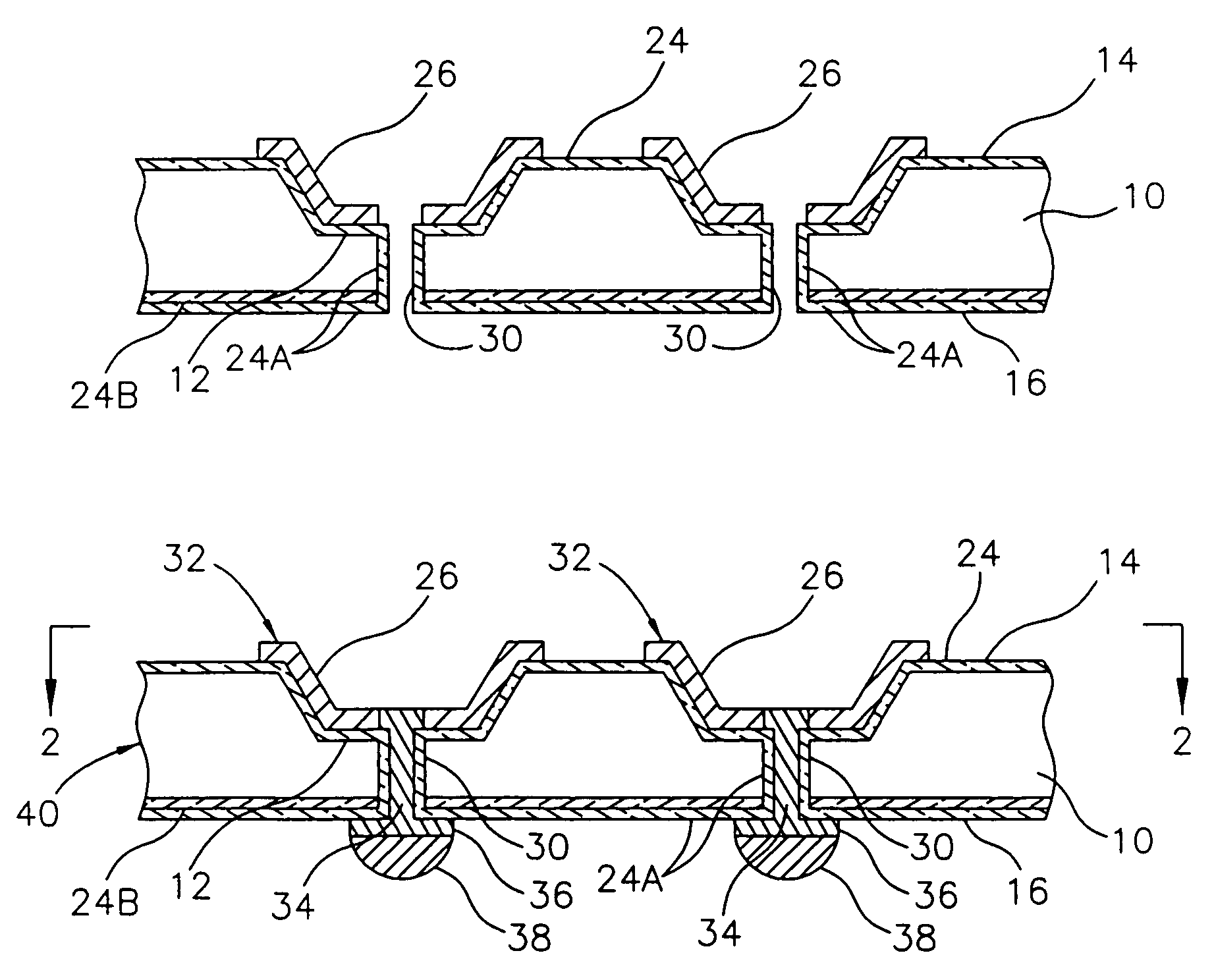
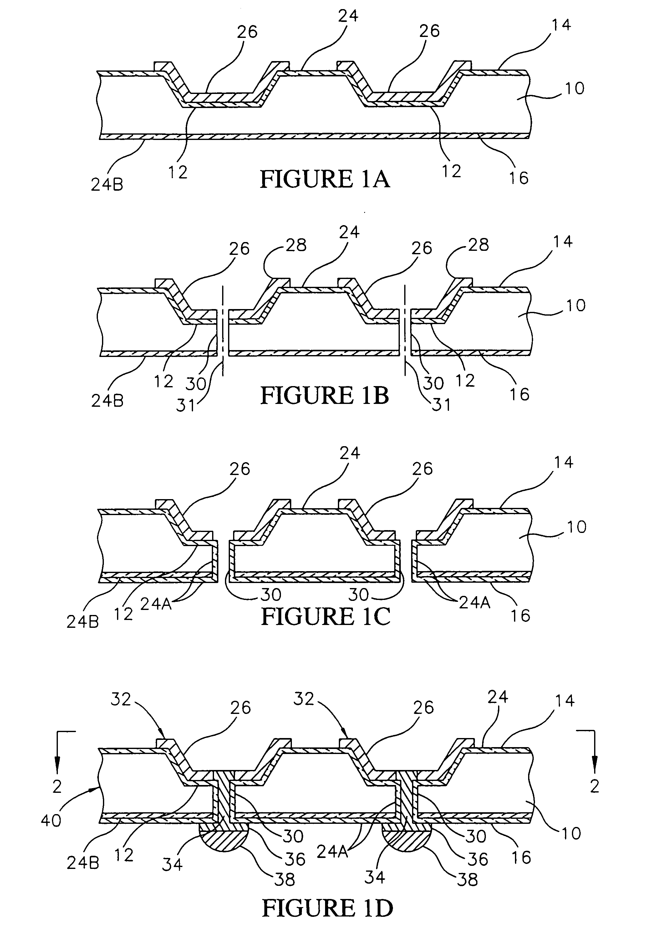
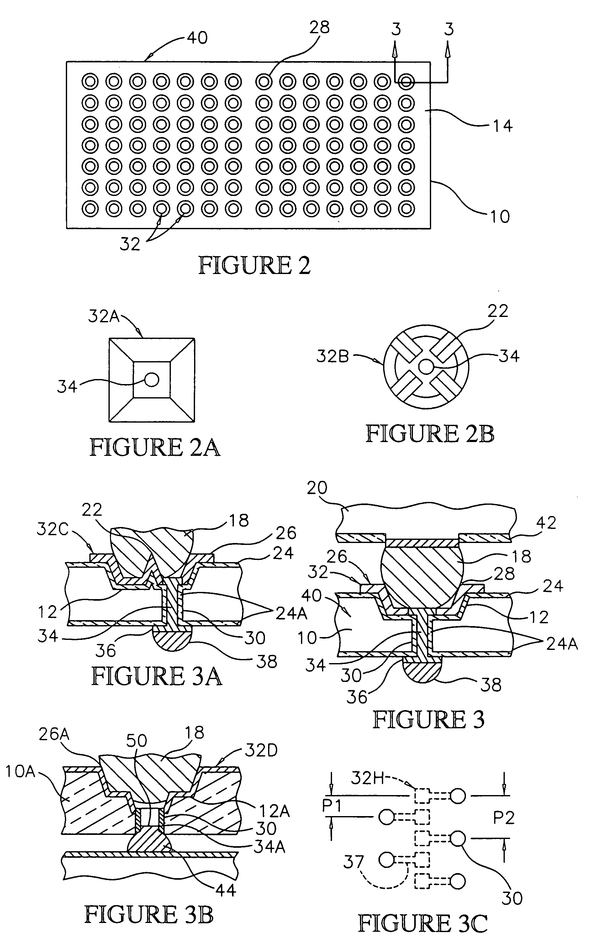
[0035]Referring to FIGS. 1A–1D, steps in a method for fabricating an interconnect in accordance with the invention are illustrated. As shown in FIG. 1A, a substrate 10 can be provided. Preferably, the substrate 10 comprises a wafer of material on which multiple interconnects will be fabricated using semiconductor circuit fabrication techniques, and then singulated by cutting the wafer. Such a process is referred to as a wafer level fabrication process.

[0036]In the embodiment illustrated in FIGS. 1A–1D, the substrate 10 comprises a semiconductor material such as monocrystalline silicon, germanium, silicon-on-glass, or silicon-on-sapphire. In other embodiments to be subsequently described, the substrate 10 can comprise a ceramic material, or of a glass filled resin material, such as FR-4.

[0037]The substrate 10 includes a face side 14 and an opposing backside 16. The face side 14 and backside 16 of the substrate are planar surfaces generally parallel to one another. A representative th...


PUM


Abstract

An interconnect for semiconductor components such as dice, wafers and chip scale packages is provided. The interconnect includes a substrate, and patterns of contacts formed on a face side of the substrate adapted to electrically engage external contacts (e.g., bond pads, solder bumps) on the components. The interconnect also includes insulated conductive members through the substrate, which provide direct electrical paths from the interconnect contacts to a backside of the substrate. The conductive members can be formed by laser machining openings in the substrate, and then filling the openings with a conductive material (e.g., metal, conductive polymer). The conductive members can also include pads with contact balls, configured for electrical interface with a test apparatus, such as test carrier or wafer handler. The interconnect can be used to construct test systems for testing semiconductor components, or to construct chip scale packages and multi chip modules.

Description

CROSS REFERENCE TO RELATED APPLICATIONS[0001]This application is a continuation of Ser. No. 09 / 961,646, filed Sep. 25, 2001, U.S. Pat. No. 6,833,613 B1, which is a division of Ser. No. 09 / 385,606, filed Aug. 30, 1999, U.S. Pat. No. 6,294,837 B1, which is a division of Ser. No. 08 / 993,965, filed Dec. 18, 1997, U.S. Pat. No. 6,107,109.[0002]This application is related to Ser. No. 10 / 316,349, filed Dec. 11, 2002, U.S. Pat. No. 6,903,433 B2, to Ser. No. 10 / 035,355, filed Jan. 4, 2002, U.S. Pat. No. 6,620,731 B1, to Ser. No. 10 / 820,674, filed Apr. 8, 2004, and to Ser. No. 10 / 998,269 filed Nov. 26, 2004.FIELD OF THE INVENTION[0003]This invention relates generally to semiconductor manufacture, and specifically to an interconnect having laser machined contacts for electrically engaging external contacts on semiconductor components such as dice, wafers and chip scale packages.BACKGROUND OF THE INVENTION[0004]Semiconductor components include external contacts that allow electrical connections...

Claims


Application Information

Patent Timeline
Patent Type & Authority Patents(United States)
IPC IPC(8): H01L21/44H01L21/48H01L21/60H01L21/768H01L23/13H01L23/498H01L23/538H01L25/10H05K1/03H05K1/11H05K3/00
CPCH01L21/486H01L23/13H01L23/49827H01L23/5389H01L24/16H01L24/75H01L24/81H01L25/105H05K1/112H01L21/76898H01L2224/16235H01L2224/13099H01L2224/13111H01L2224/13144H01L2224/13147H01L2224/16H01L2224/75H01L2224/81801H01L2224/82039H01L2924/01004H01L2924/01013H01L2924/0102H01L2924/01022H01L2924/01027H01L2924/01029H01L2924/01032H01L2924/01039H01L2924/01042H01L2924/01046H01L2924/01047H01L2924/01073H01L2924/01074H01L2924/01077H01L2924/01078H01L2924/01079H01L2924/01082H01L2924/09701H01L2924/14H01L2924/15311H05K1/0306H05K3/0029H05K3/0032H05K2201/09472H05K2201/0959H05K2201/09827H05K2201/09845H05K2201/10674H05K2201/10734H01L2924/01005H01L2924/01006H01L2924/01033H01L2924/0105H01L2924/01072H01L2924/01087H01L2924/014H01L2225/1023H01L2225/1058H01L2224/16225H01L2224/48227H01L2924/12042H01L2224/05571H01L2224/05573H01L2924/00014H01L24/03H01L2224/0615H01L24/05H01L2924/00H01L2224/05599
Inventor AKRAM, SALMANFARNWORTH, WARREN M.WOOD, ALAN G.
Owner ROUND ROCK RES LLC
Why Eureka
Try Eureka