Crystallization apparatus, crystallization method, and phase shifter

a crystallization method and crystallization apparatus technology, applied in the field of crystallization apparatus, crystallization method, and phase shifter applied to a nonsingle crystallized semiconductor film, can solve the problems of inability to two-dimensionally control the region where the crystal grain is formed, the number of crystal grain boundaries fluctuating within the channel region,

Inactive Publication Date: 2006-02-21
ADVANCED LCD TECH DEVMENT CENT
View PDF6 Cites 34 Cited by
  • Summary
  • Abstract
  • Description
  • Claims
  • Application Information

AI Technical Summary

Benefits of technology

[0012]An object of the present invention is to provide a crystallization apparatus, crystallization method, and phase shifter, which can two-dimensionally control a region where a single-crystal grain is formed.

Problems solved by technology

When the poly-silicon is used to form a small-sized transistor, this raises a problem that the number of crystal grain boundaries fluctuates within a channel region.
In other words, in the conventional art, it has been impossible to specify the creation point of the crystal nucleus, and it has also been impossible to two-dimensionally control a region where the crystal grain is formed.

Method used


Image

  • Crystallization apparatus, crystallization method, and phase shifter
  • Crystallization apparatus, crystallization method, and phase shifter
  • Crystallization apparatus, crystallization method, and phase shifter

Examples


first embodiment

[0034]A crystallization apparatus according to the present invention will be described hereinafter with reference to the accompanying drawings.

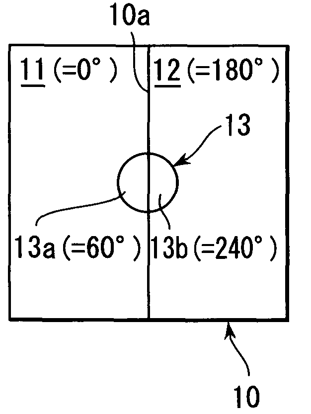
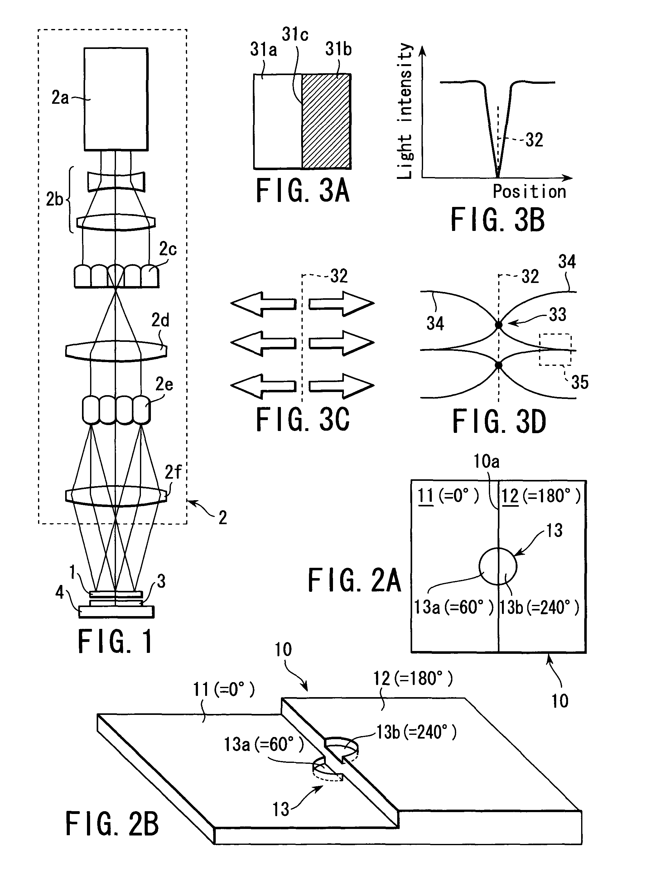
[0035]FIG. 1 is a diagram schematically showing the configuration of the crystallization apparatus. The crystallization apparatus includes an illumination system 2 which illuminates a phase shifter 1. The illumination system 2 includes a KrF excimer laser source 2a which supplies a laser light having a wavelength, for example, of 248 nm. It is to be noted that the light source 2a may be replaced by another appropriate light source such as an XeCl excimer laser source. The laser light from the light source 2a is enlarged via a beam expander 2b and subsequently incident upon a first fly eye lens 2c.

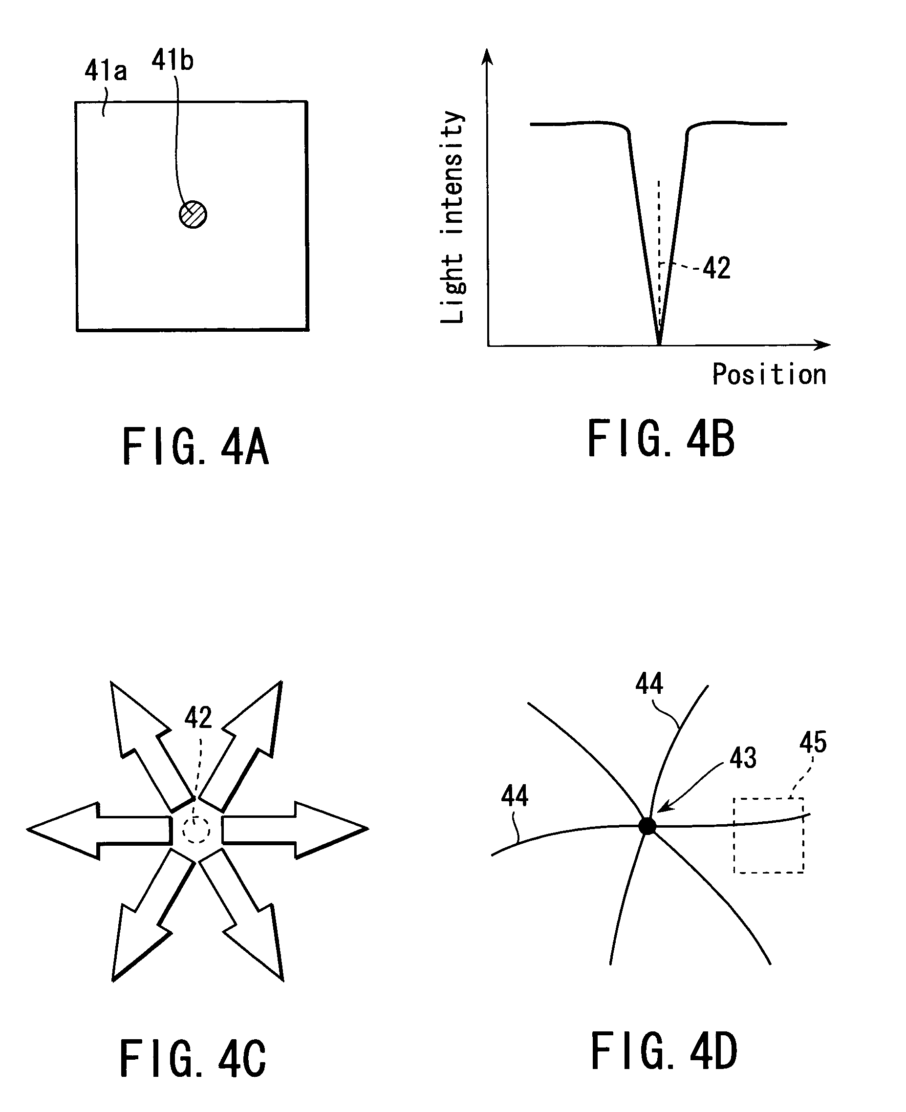
[0036]The first fly eye lens 2c has a focal surface provided on the rear side thereof and serves as a plurality of light sources. Luminous fluxes from these light sources illuminate an incidence surface of a second fly eye lens 2e via a first conden...

second embodiment

[0066]In the second embodiment, the optical imaging system 5 is disposed between the phase shifter 1 and sample substrate 3 to locate the phase shifter 1 and sample substrate 3 at the optically conjugated positions. In other words, the sample substrate 3 is set in a plane optically conjugated with the phase shifter 1 (image plane of the optical imaging system 5). An aperture diaphragm unit 5a is disposed in an iris plane of the optical imaging system 5. The aperture diaphragm unit 5a includes a plurality of aperture diaphragms different from one another in the size of the aperture (light transmission portion), and these aperture diaphragms can be changed with respect to an optical path.

[0067]Moreover, the aperture diaphragm unit 5a may also be formed of an iris diaphragm that can continuously change the size of the aperture. In any case, the size of the aperture of the aperture diaphragm unit 5a (numerical aperture NA on the imaging side of the optical imaging system 5) is set to ob...


PUM

PropertyMeasurementUnit
wavelengthaaaaaaaaaa
refractive indexaaaaaaaaaa

Abstract

A crystallization apparatus includes an illumination system which applies illumination light for crystallization to a non-single-crystal semiconductor film, and a phase shifter which includes first and second regions disposed to form a straight boundary and transmitting the illumination light from the illumination system by a first phase retardation therebetween, and phase-modulates the illumination light to provide a light intensity distribution having an inverse peak pattern that light intensity falls in a zone of the non-single-crystal semiconductor film containing an axis corresponding to the boundary. The phase shifter further includes a small region which extends into at least one of the first and second regions from the boundary and transmits the illumination light by a second phase retardation with respect to the at least one of the first and second regions.

Description

CROSS-REFERENCE TO RELATED APPLICATIONS[0001]This application is based upon and claims the benefit of priority from the prior Japanese Patent Application No. 2002-262249, filed Sep. 9, 2002, the entire contents of which are incorporated herein by reference.BACKGROUND OF THE INVENTION[0002]1. Field of the Invention[0003]The present invention generally relates to a crystallization apparatus, crystallization method, and phase shifter applied to a non-single-crystal semiconductor film such as a polycrystalline or amorphous semiconductor film, particularly to a crystallization apparatus, crystallization method, and phase shifter for modulating a phase of laser light to be applied to the non-single-crystal semiconductor film in the crystallization.[0004]2. Description of the Related Art[0005]Materials of thin film transistors (TFT) for use as switching devices for controlling voltages to be applied to pixels, for example, of a liquid crystal display (LCD) have heretofore been roughly divi...

Claims


Application Information

Patent Timeline
Patent Type & Authority Patents(United States)
IPC IPC(8): C30B5/00G03F1/00H01L21/20B23K26/073G03F1/26G03F1/68G03F7/20H01L21/268H01L21/336H01L29/786
CPCB23K26/0656B23K26/073B23K26/0734G02B5/02G02B5/3083H01L29/66757H01L29/78675G03F1/34G03F1/28Y10T117/10H01L21/02532H01L21/02678H01L21/02686H01L27/1285B23K26/066H01L21/268
Inventor TANIGUCHI, YUKIOMATSUMURA, MASAKIYOYAMAGUCHI, HIROTAKANISHITANI, MIKIHIKOTSUJIKAWA, SUSUMUKIMURA, YOSHINOBUJYUMONJI, MASAYUKI
Owner ADVANCED LCD TECH DEVMENT CENT
Why Eureka
Try Eureka